

Methods of fabricating shield plates for reduced field coupling in nonvolatile memory
a shield plate and field coupling technology, applied in the direction of semiconductor devices, instruments, electrical equipment, etc., can solve the problems of reducing the available separation between adjacent states, erroneous reading of data stored therein, etc., and achieve the effect of reducing coupling
- Summary
- Abstract
- Description
- Claims
- Application Information
AI Technical Summary
Benefits of technology
Problems solved by technology
Method used
Image

Examples
Embodiment Construction
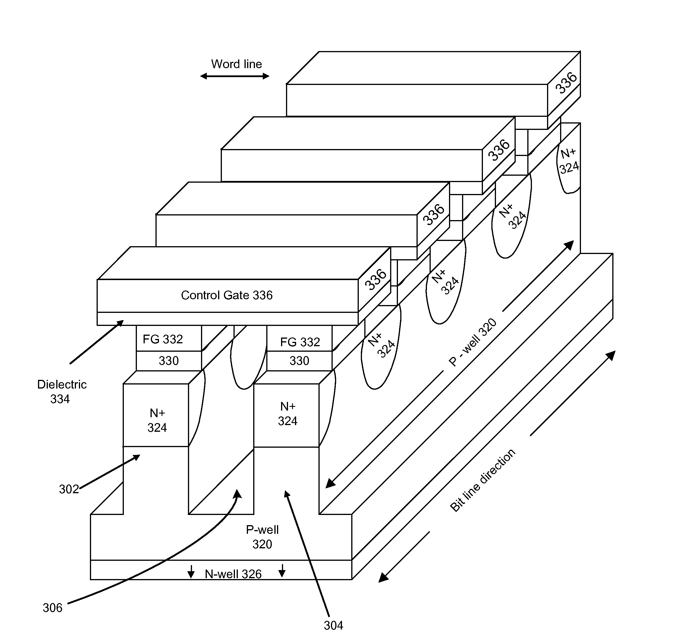
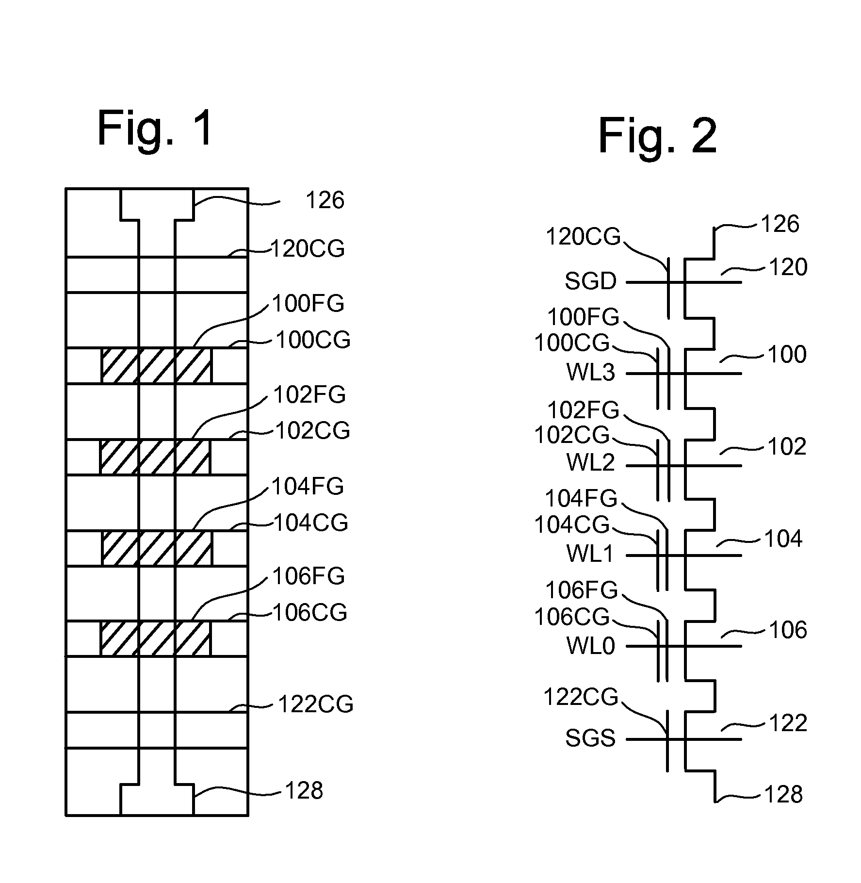
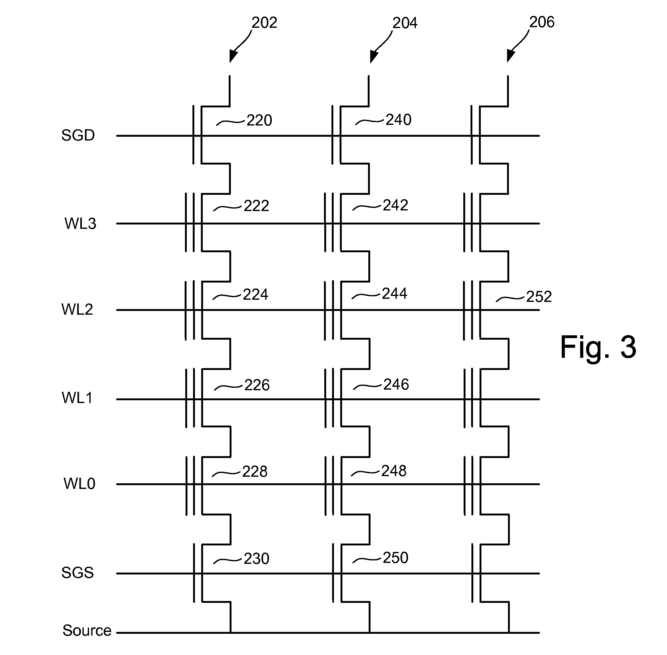
[0034]FIG. 1 is a top view showing one NAND string. FIG. 2 is an equivalent circuit thereof. Shielding and isolation techniques in accordance with embodiments are presented with respect to nonvolatile flash memory, specifically NAND type flash memory, for purposes of explanation. It will be appreciated by those of ordinary skill in the art, however, that the techniques set forth are not so limited and can be utilized in many fabrication processes to fabricate various types of integrated circuits. For example, these techniques can be used to fabricate NOR type memories or other devices where shielding is needed between neighboring charge storage regions.
[0035]The NAND string depicted in FIGS. 1 and 2 includes four transistors 100, 102, 104 and 106 in series and sandwiched between a first select gate 120 and a second select gate 122. Select gate 120 connects the NAND string to a bit line via bit line contact 126. Select gate 122 connects the NAND string to a common source line via sou...
PUM
 Abstract
Description
Claims
Application Information