

Area-Efficient Gated Diode Structure and Method of Forming Same
a gated diode and area-efficient technology, applied in the field of area-efficient gated diodes, can solve the problems of undesirable large layout area, double overlap capacitance, and inability to achieve area-efficient implementation of gated diodes, and achieve the effect of increasing the planar layout area enhancing area efficiency, and beneficially increasing the capacitance of the gated diod
- Summary
- Abstract
- Description
- Claims
- Application Information
AI Technical Summary
Benefits of technology
Problems solved by technology
Method used
Image

Examples
Embodiment Construction
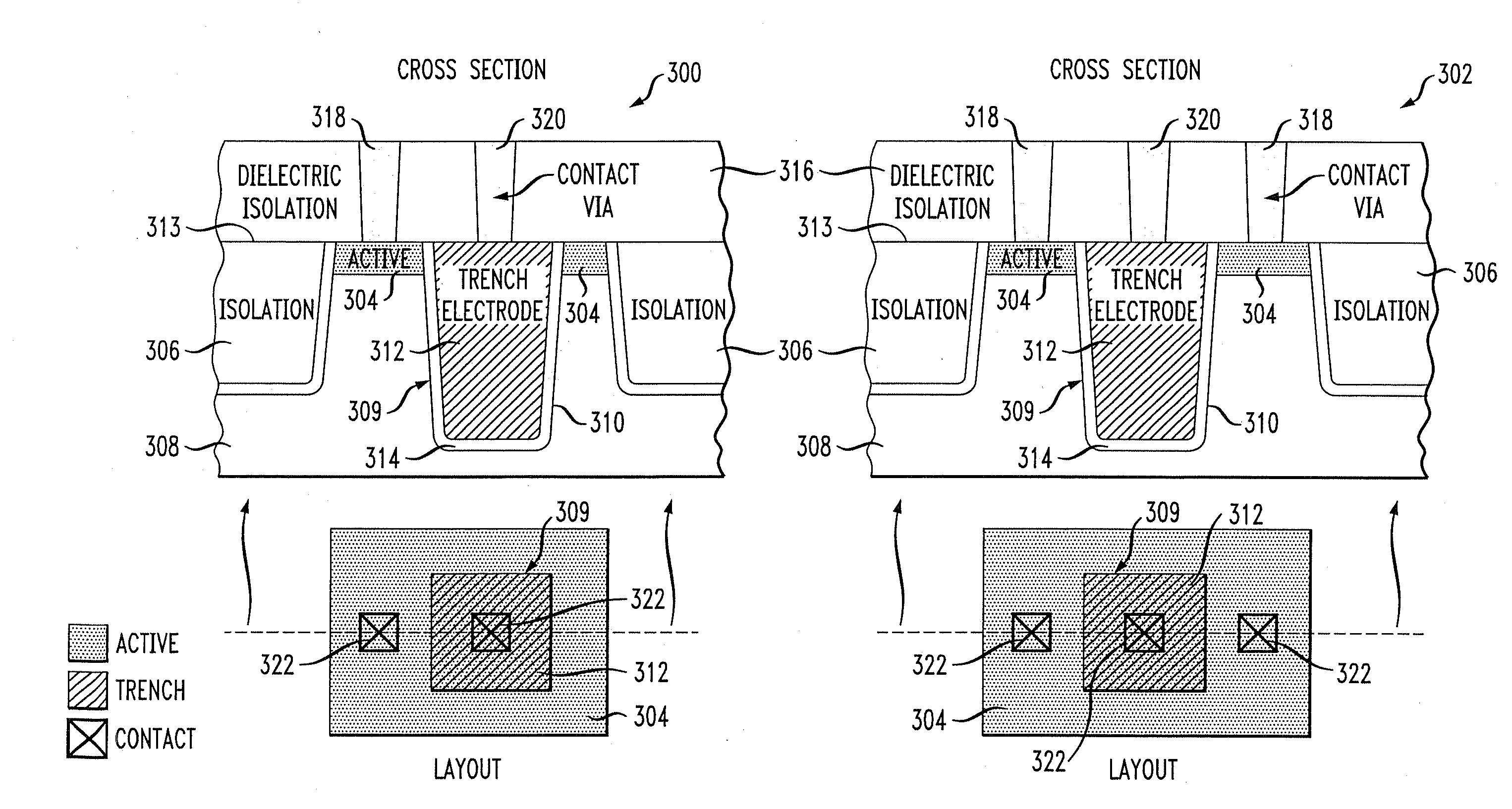
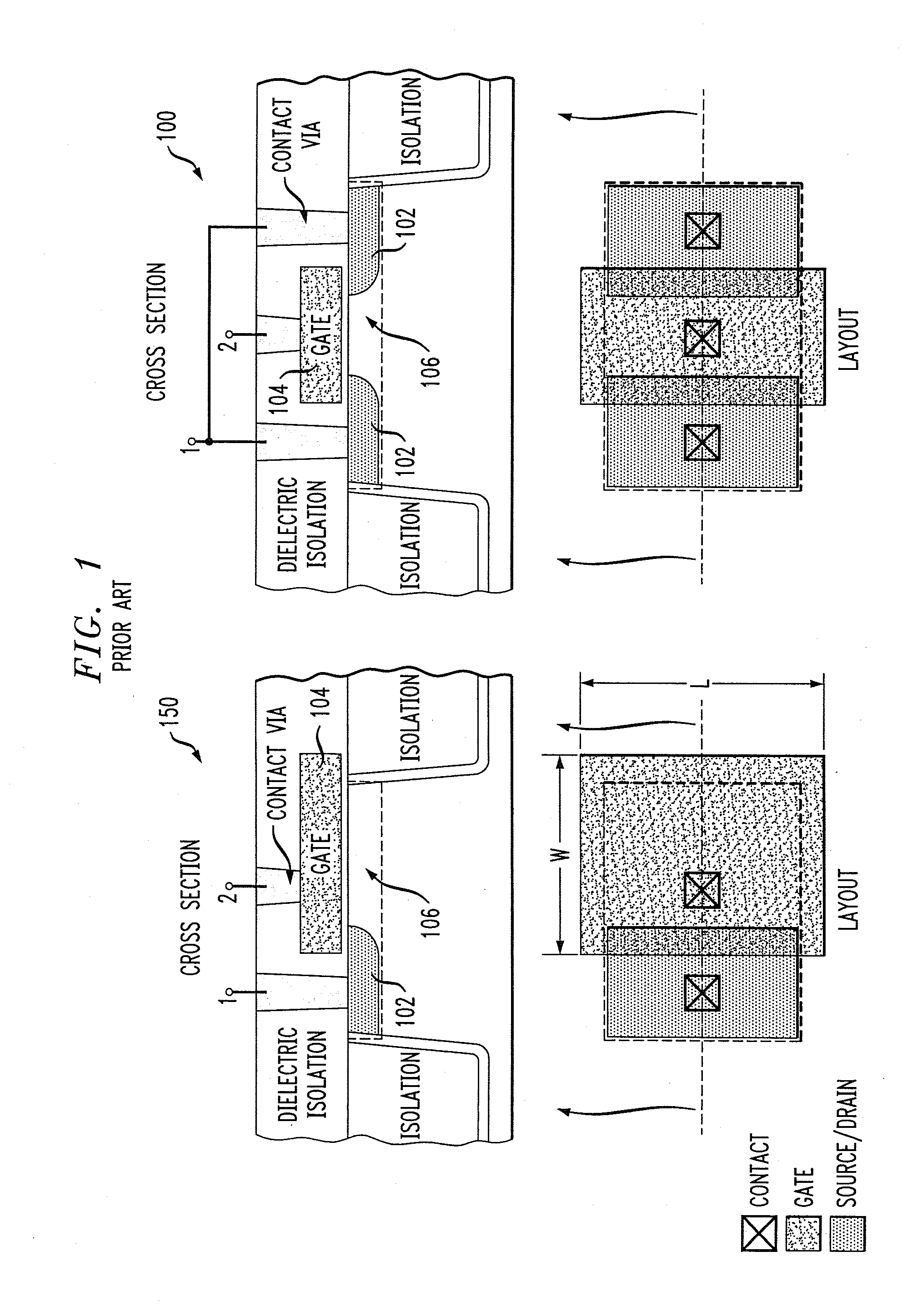
[0024]The present invention will be described herein in the context of illustrative trench gated diode structures. It should be understood, however, that the present invention is not limited to this or any other particular semiconductor structure. Rather, the invention is more generally applicable to techniques for beneficially increasing a capacitance of a gated diode without significantly increasing a layout area of the gated diode. Although implementations of the present invention are described herein with specific reference to a CMOS fabrication process, it is to be understood that the invention is not limited to such a fabrication process, and that other suitable fabrication processes (e.g., bipolar, BiCMOS, etc.), may be similarly employed, as will be apparent to those skilled in the art.
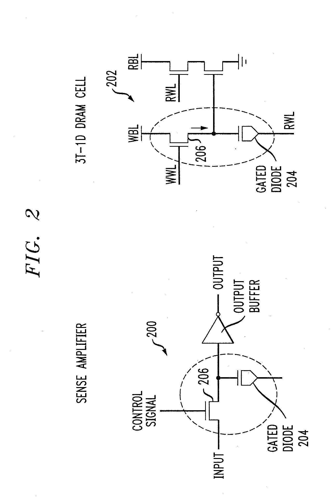
[0025]As previously stated, an advantage of a gated diode is that it is particularly well suited for use in high performance and low voltage circuit applications, such as, for example, sense a...
PUM
 Abstract
Description
Claims
Application Information