Method of Forming Vertical Contacts in Integrated Circuits

a technology of integrated circuits and vertical contacts, which is applied in the direction of semiconductor devices, semiconductor/solid-state device details, electrical apparatus, etc., can solve the problems of non-ideal patterning of mtj elements, non-ideal mtj shapes, and irreproducible device behavior, so as to reduce the cost and complexity of manufacturing the integrated circui

Inactive Publication Date: 2008-07-10
GLOBALFOUNDRIES INC
View PDF16 Cites 17 Cited by
  • Summary
  • Abstract
  • Description
  • Claims
  • Application Information

AI Technical Summary

Benefits of technology

[0007]In accordance with an illustrative embodiment of the invention, an integrated circuit comprises an MTJ that occupies a level between an upper metallization level and a lower metallization level. Vertical contacts are formed between the upper metallization level and the MTJ and between the upper metallization level and the lower metallization level using processing methods in accordance with aspects of the invention. Advantageously, the vertical contact to the MTJ and the vertical contact to the lower metallization level may be formed at the same time, thereby substantially reducing the cost and complexity of manufacturing the integrated circuit.

Problems solved by technology

The patterning of magnetic tunnel junctions (MTJs) and the formation of vertical contacts between MTJs and metal interconnects remain challenging processes in the formation of magnetoresistive random access memory (MRAM) integrated circuits.
Unfortunately, the above-described approach to patterning an MTJ and electrically coupling the MTJ to a metal interconnect may result in non-ideal patterning of the MTJ element.
The RIE process may also form an undesirable “foot” on the MTJ due to shadowing effects from the thick hard mask.
Moreover, sidewall roughness from the use of the relatively thick hard mask layer may result in non-ideal MTJ shapes and irreproducible device behavior.
As a result, the conventional manner of patterning an MTJ and coupling the MTJ to a metal interconnect may have a severe impact on the electrical and magnetic performance of the MTJ.

Method used


Image

  • Method of Forming Vertical Contacts in Integrated Circuits
  • Method of Forming Vertical Contacts in Integrated Circuits
  • Method of Forming Vertical Contacts in Integrated Circuits

Examples


Embodiment Construction

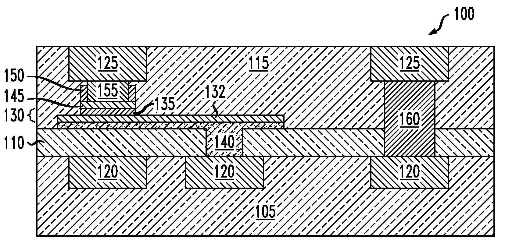
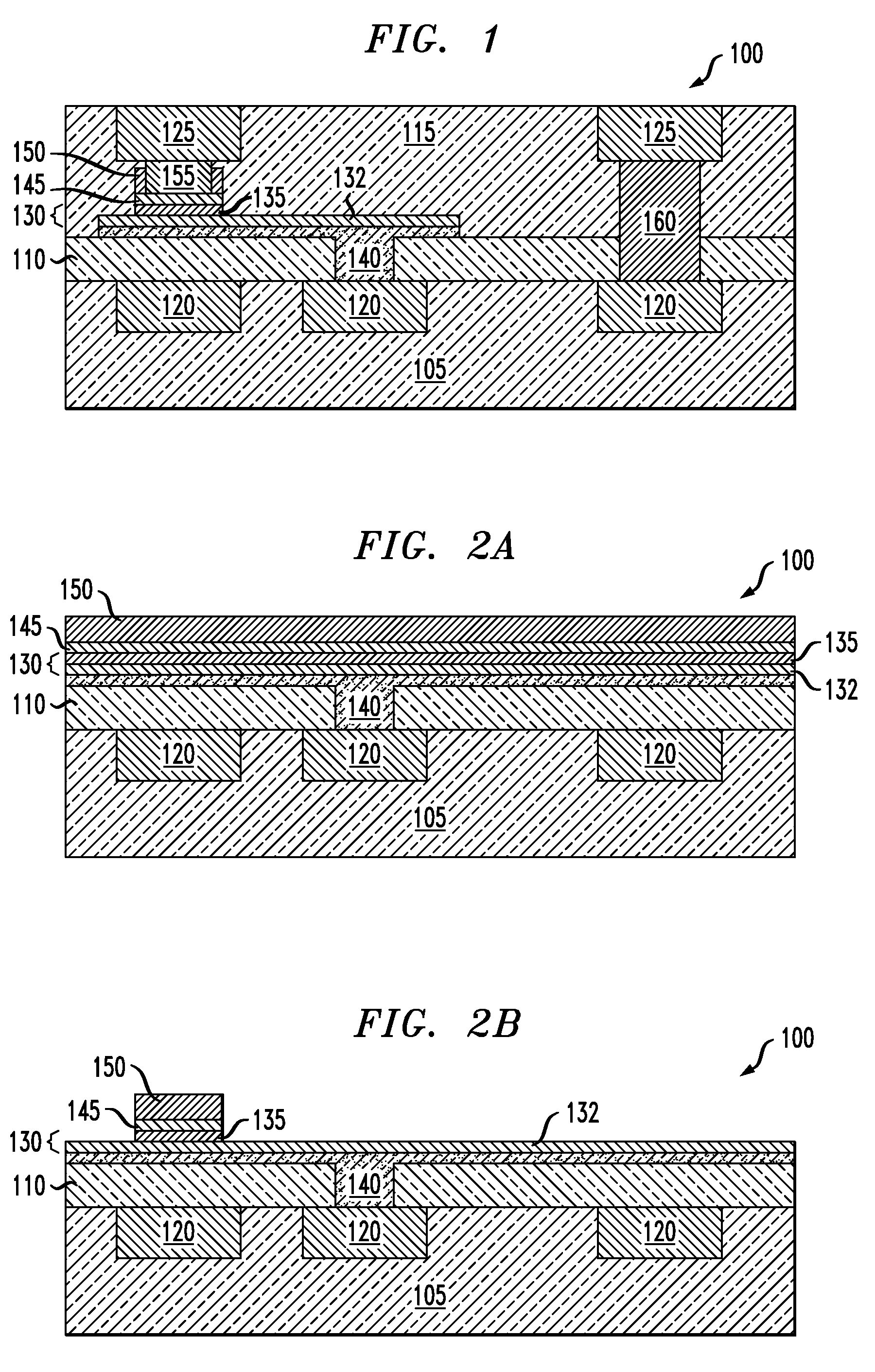
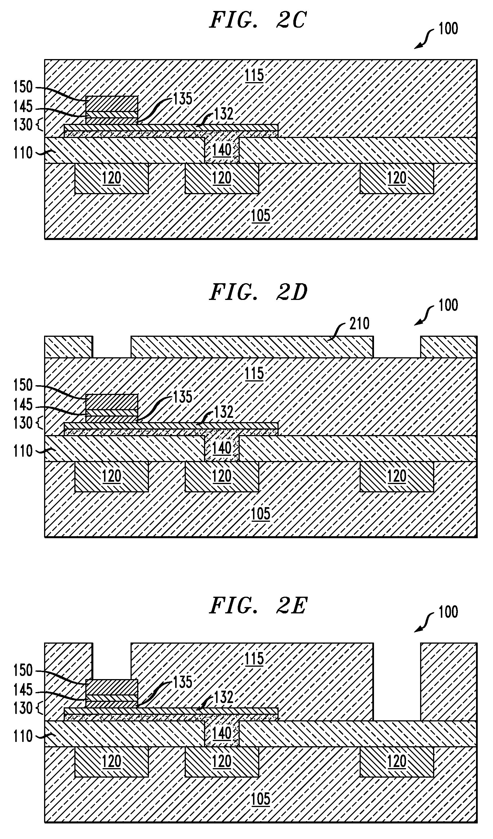
[0015]The present invention will be described with reference to illustrative embodiments. For this reason, numerous modifications can be made to these embodiments and the results will still come within the scope of the invention. For instance, while the illustrative embodiments describe integrated circuits comprising MTJs and various metallization features, the invention is not limited to these particular features. No limitations with respect to the specific embodiments described herein are intended or should be inferred.

[0016]Although combined in a novel manner, most of the processing steps described herein (e.g., deposition steps, etching steps and photolithography steps) are frequently performed in conventional semiconductor processing, and, as result, will be familiar to one skilled in that art. Moreover, details of the individual processing steps used to fabricate semiconductor devices described herein may be found in a number of publications, for example, S. Wolf and R. N. Tau...


PUM


Abstract

A method of forming vertical contacts in an integrated circuit that couple one or more metal lines in a given metallization level to first and second features occupying different levels in the integrated circuit comprises various processing steps. A first etch stop layer is formed overlying at least of portion of the first feature while a second etch stop layer is formed overlying at least a portion of the second feature. An ILD layer is formed overlying the first and second etch stop layers. A photolithographic mask is formed overlying the ILD layer. The photolithographic mask defines a first opening over the first feature and a second opening over the second feature. A first etch process etches a first hole in the ILD layer through the first opening in the photolithographic mask that lands on the first etch stop layer and etches a second hole in the ILD layer through the second opening that lands on the second etch stop layer. Subsequently, a second etch process further etches the first hole so that it lands on the first feature.

Description

FIELD OF THE INVENTION[0001]The present invention is directed generally to integrated circuits, and, more particularly, to forming vertical contacts in integrated circuits.BACKGROUND OF THE INVENTION[0002]The patterning of magnetic tunnel junctions (MTJs) and the formation of vertical contacts between MTJs and metal interconnects remain challenging processes in the formation of magnetoresistive random access memory (MRAM) integrated circuits. In one method, an MTJ is formed and electrically coupled to an overlying metal interconnect by depositing a relatively thick metallic hard mask layer on top of the many layers of magnetic and nonmagnetic materials that will make up the MTJ. This hard mask layer is patterned into the shape of the desired MTJ by conventional photolithography and reactive ion etching (RIE). The MTJ layers are then patterned using the patterned hard mask layer as a self-aligned mask structure. Afterwards, an interlayer dielectric (ILD) layer is conformally deposite...

Claims


Application Information

Patent Timeline
Patent Type & Authority Applications(United States)
IPC IPC(8): H01L23/52H01L21/4763
CPCH01L21/76807H01L43/12H01L21/76816H10N50/01
Inventor ASSEFA, SOLOMONGAIDIS, MICHAEL C.HUMMEL, JOHN P.KANAKASABAPATHY, SIVANANDA K.
Owner GLOBALFOUNDRIES INC
Why Eureka
Try Eureka