Time Based Driver Output Transition (Slew) Rate Compensation

a driver output and transition rate technology, applied in the field of minimization of driver output slew rate variation, can solve the problems of unfavorable timing and signal integrity implications of optimal edge rate, unfavorable timing and signal integrity class, and unfavorable compensation

Active Publication Date: 2008-07-10
MARVELL ASIA PTE LTD
View PDF17 Cites 12 Cited by
  • Summary
  • Abstract
  • Description
  • Claims
  • Application Information

AI Technical Summary

Problems solved by technology

Deviating from this optimal edge rate typically has unfavorable timing and signal integrity implications.
Moreover, this class of timing and signal integrity problems will become even more pronounced in the future as both buss operating frequencies and silicon device parametric variations are expected to increase.
Further, as the reference circuit is much less complex than the compensated circuit and measures a DC variable parameter to compensate a quasi-related AC variable parameter, the compensation is not optimum.
Using these correlative techniques renders this task virtually impossible with the required degree of accuracy.
Other deficiencies in this technique arise in that only one or two reference circuits are used to determine the PVT bit settings for potentially hundreds of drivers across the chip completely ignoring output slew variation caused by across chip, load and local power supply variation.

Method used


Image

  • Time Based Driver Output Transition (Slew) Rate Compensation
  • Time Based Driver Output Transition (Slew) Rate Compensation
  • Time Based Driver Output Transition (Slew) Rate Compensation

Examples


Embodiment Construction

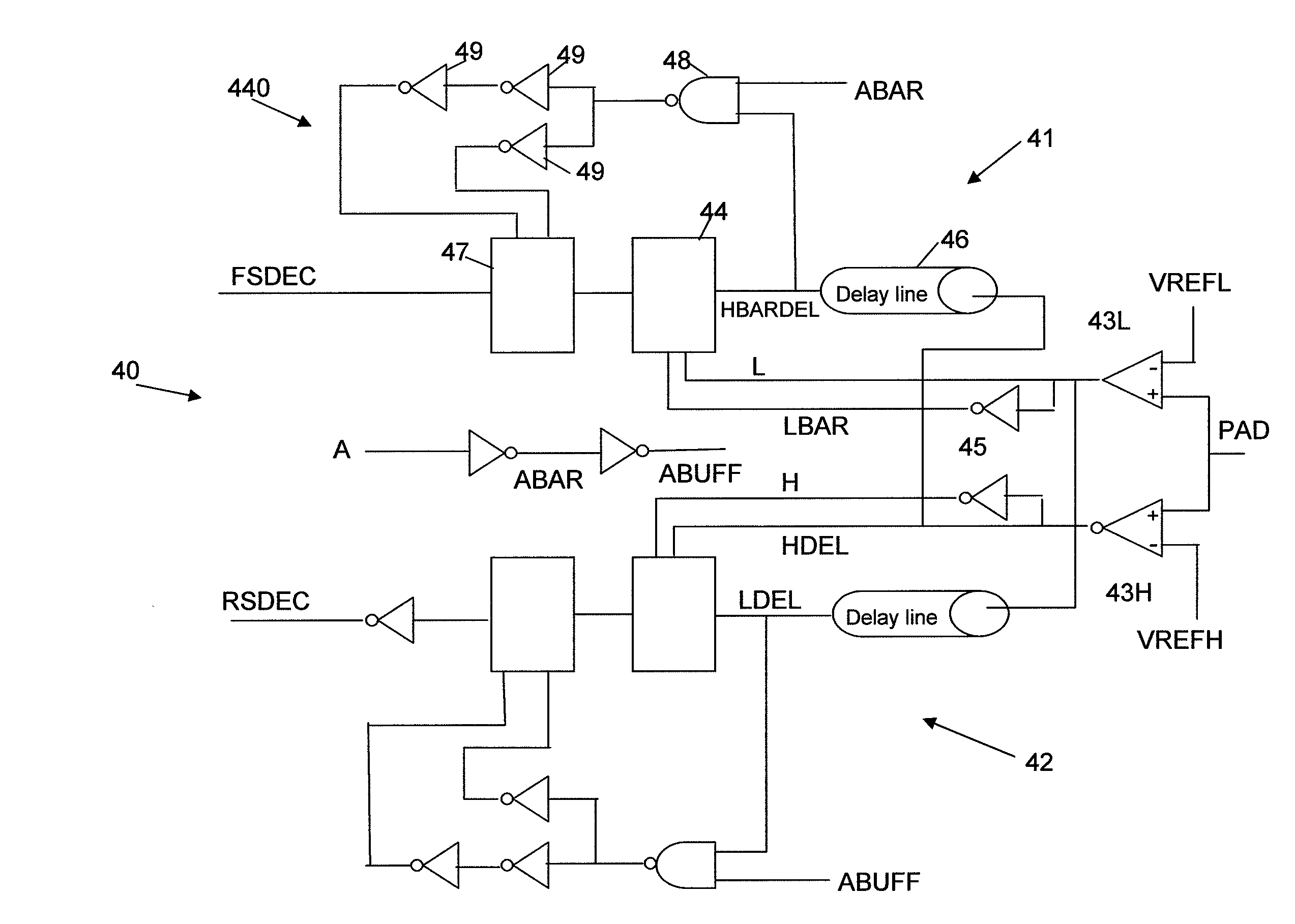
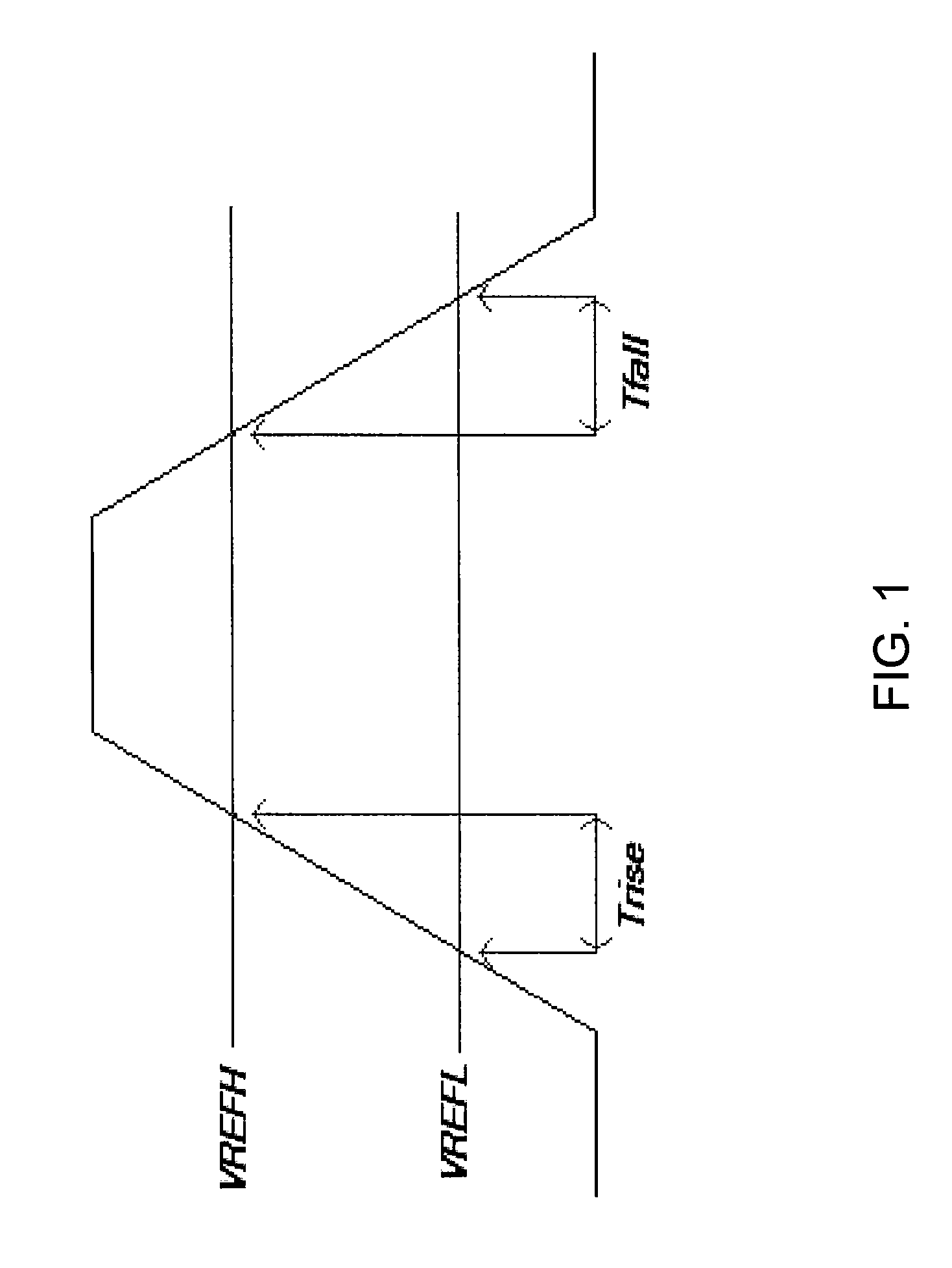
[0018]The invention is directed to a method and apparatus to effectively minimize driver output slew rate variation. In accordance with the invention, the slew of each driver can be directly measured and controlled.

[0019]While the prior art PVT Correlation technique discussed above provides a certain degree of output slew rate compensation, it has been demonstrated in practice that when tight tolerances are required, this technique simply cannot deliver the required accuracy. The inventors have found that the major flaw in the correlation technique is that the parameter of interest, driver output slew rate, is indirectly compensated instead of actually being both measured and controlled directly. According to the invention, the controlled parameter is the measured parameter, and the control of the parameter requires a near perfect reference and measurement technique.

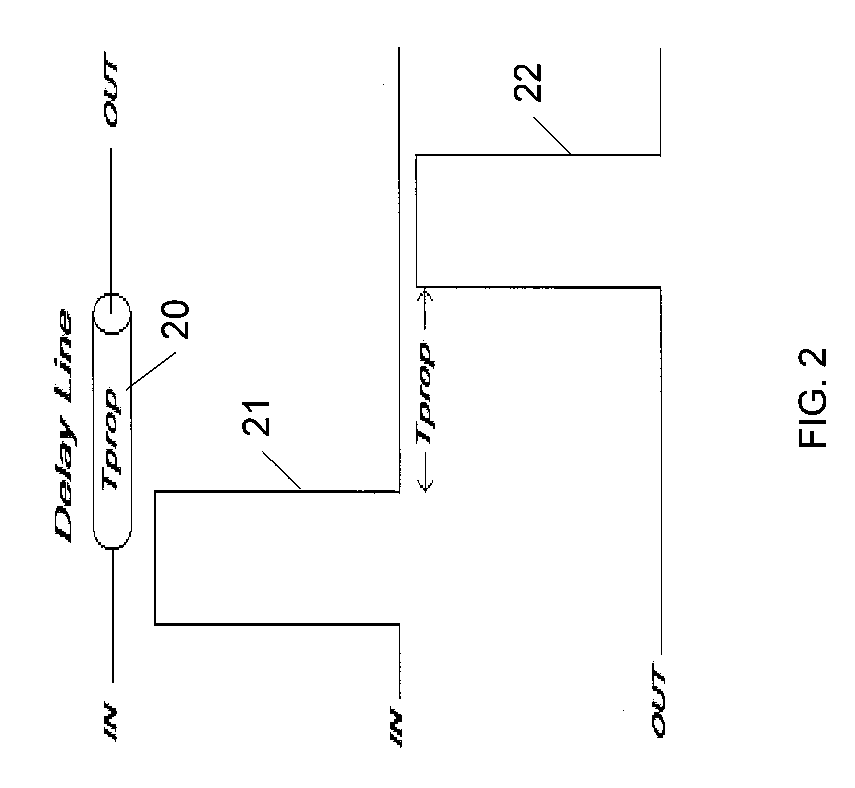
[0020]In accordance with the invention, a circuit is provided to implement the technique to sample / measure, compare an...


PUM


Abstract

Apparatus and method for controlling the driver output slew rate. The apparatus includes a driver circuit having an input signal and an output signal, where the driver circuit is structured and arranged to facilitate control of the slew rate of the output signal. A delay circuit having a time delay proportional to a desired transition time of the driver output signal is coupled to the output of the driver circuit. A first comparator detects when the driver output signal rises through a specified level, and a second comparator detects when the driver output falls through a second specified level. A phase detector is coupled to outputs of the first and second comparators and an output of the delay circuit for aligning the phases of the comparator outputs and the delayed comparator outputs by adjusting the driver output slew rate.

Description

FIELD OF THE INVENTION[0001]The invention generally relates to a method and apparatus to minimize driver output slew rate variation.BACKGROUND OF INVENTION[0002]Many of today's I / O driver specifications require very small output slew rate variation; particularly specifications for multi-I / O busses. Through network analysis, an optimal output edge rate can be determined to minimize Inter Symbol Interference (ISI) and signal propagation time, and thereby increase the maximum operating frequency of the system. Deviating from this optimal edge rate typically has unfavorable timing and signal integrity implications.[0003]As is known among I / O and System designers, driver output slew rate variation is primarily a function of the driver circuit topology, varying operating conditions, such as voltage and temperature, silicon process variation and the particular application load network. As higher operating frequencies and stricter timing requirements have forced tighter output slew variatio...

Claims


Application Information

Patent Timeline
Patent Type & Authority Applications(United States)
IPC IPC(8): H03K5/12
CPCH03K19/017581H03K19/00369
Inventor BUCOSSI, WILLIAM LDEBRITA, ALBERT A.
Owner MARVELL ASIA PTE LTD
Why Eureka
Try Eureka