Laser light source device, and image device using the same

a technology of laser light source and image device, which is applied in the direction of laser details, color television details, semiconductor lasers, etc., can solve the problems of increasing manufacturing costs and achieve the effect of suppressing the scale of the power supply circui

Inactive Publication Date: 2008-07-10
COLUMBIA PEAK VENTURES LLC
View PDF1 Cites 23 Cited by
  • Summary
  • Abstract
  • Description
  • Claims
  • Application Information

AI Technical Summary

Benefits of technology

[0007]An object of the present invention is to suppress the scale of the power supply circuit from becoming very large for the laser light source device equipped with a wavelength conversion component. Another object of the present invention is to provide technology for which it is possible to drive using a preferable control mode according to the application.

Problems solved by technology

Because of that, to make it possible to supply more power, the scale of the power supply circuit becomes larger, and by using a component with high current drivability as the component constituting the power supply circuit, this brings increases in manufacturing costs.

Method used


Image

  • Laser light source device, and image device using the same
  • Laser light source device, and image device using the same
  • Laser light source device, and image device using the same

Examples


first embodiment

A. First Embodiment

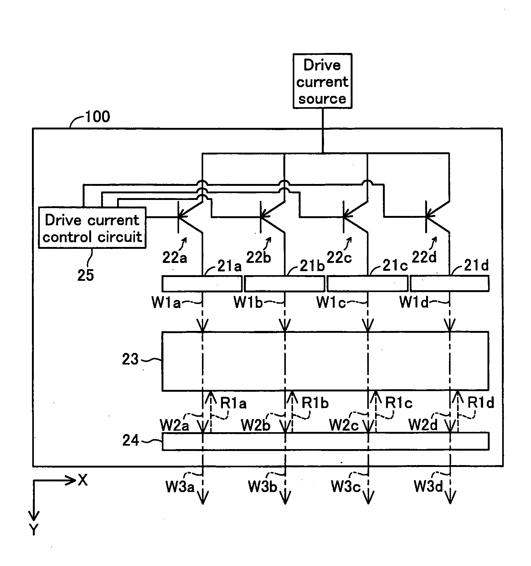
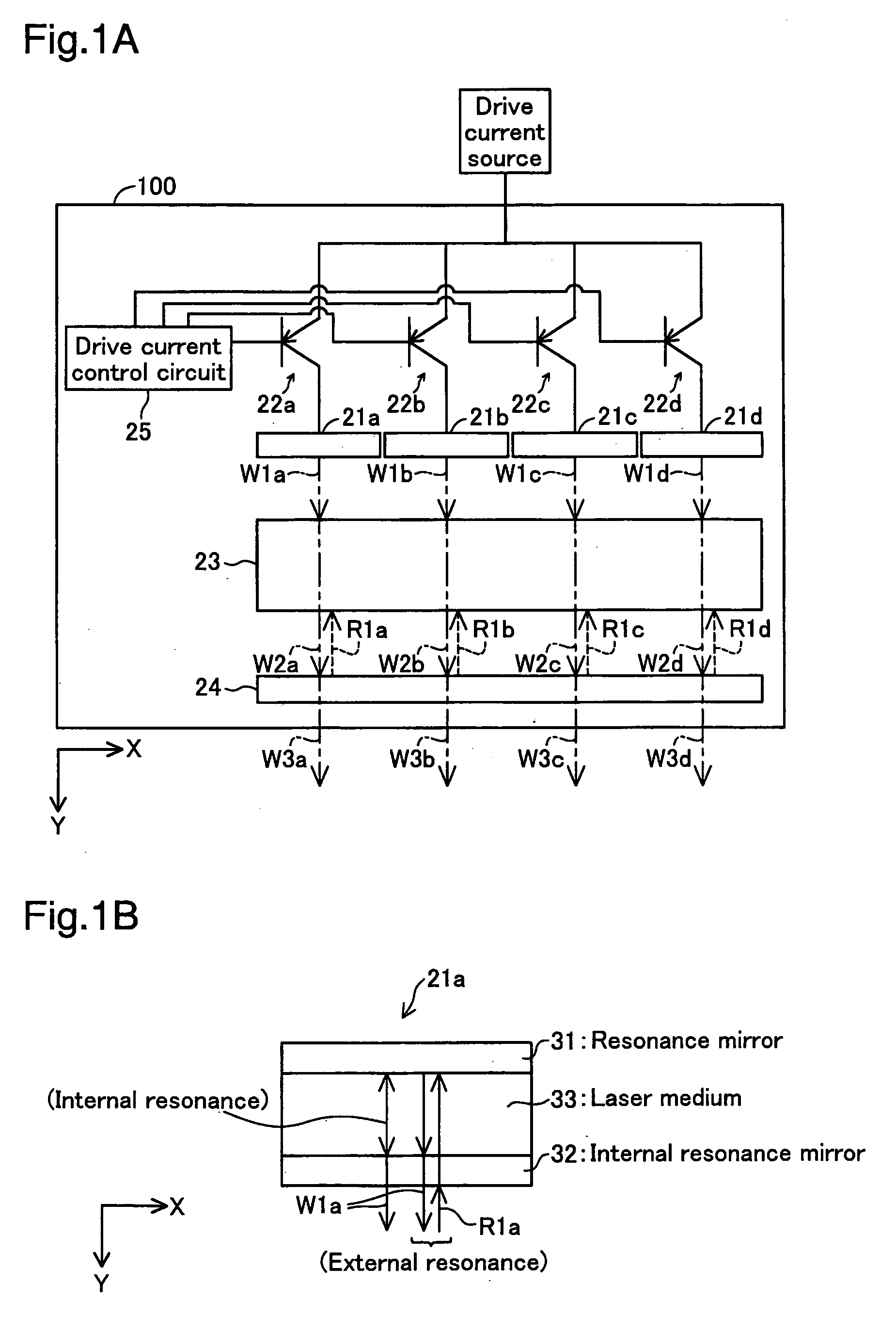
[0040]FIG. 1A is an explanatory drawing showing the schematic structure of a laser light source device as an embodiment of this invention. This laser light source device 100 is an external resonance type laser light source device, and is equipped with four semiconductor laser components 21a to 21d, transistors 22a to 22d for each semiconductor laser component 21a to 21d, a drive current control circuit 25 connected to the base electrode of each transistor 22a to 22d, a wavelength conversion component 23, and an output mirror 24. The four semiconductor laser components 21a to 21d are aligned in one row in the X axis direction, forming a one dimensional array structure. The part of the device which includes the semiconductor laser components 21a-21d, the wavelength conversion component 23, and the output mirror 24 may be referred to as a “light source section.”

[0041]FIG. 1B is an explanatory drawing showing the schematic structure of the semiconductor laser componen...

second embodiment

B. Second Embodiment

[0053]FIG. 5 is an explanatory drawing showing changes over time of the drive current for a second embodiment. The horizontal axis and vertical axis in FIG. 5 are the same as those in FIGS. 4A and 4B. Also, with FIG. 5, the changes over time of the drive current are shown for each semiconductor laser component 21a to 21d. With this embodiment, the point of the time positions of the pulses of the drive current supplied to each semiconductor laser component 21a to 21d are mutually different. This feature is different from the first embodiment, and the remainder of the constitution is the same as the first embodiment.

[0054]As shown in FIG. 5, the same as with the first embodiment, pulse form drive current is supplied to the semiconductor laser components 21a to 21d. However, in contrast to the first embodiment, the time positions of the pulses of the drive current supplied to the semiconductor laser components 21a to 21d are mutually different, and each pulse does n...

third embodiment

C. Third Embodiment

[0057]FIG. 7 is an explanatory drawing showing changes over time of the drive current for a third embodiment. The horizontal axis and vertical axis of FIG. 7 are the same as those of FIG. 6. Also, with FIG. 7, changes over time of the drive current for each of the semiconductor laser components 21a to 21d are shown. With each of the embodiments describe above, when the laser light source device is shining more brightly, both the peak current of the drive current and the duty ratio (pulse width) are made to be changed. Note that the control mode of the drive current that changes both the drive current peak current and the duty ratio in this way is hereinafter referred to as “duty ratio adjustment mode.” In contrast to this, with this embodiment, with the laser light source device, in addition to the duty ratio adjustment mode, there is also a preset control mode that changes only the peak current with the duty ratio (pulse width) left constant; this mode will be he...


PUM


Abstract

A laser light source device includes a light source section, and a drive current controller. The light source section includes a first and second fundamental light source component, and a wavelength conversion component. The first and second fundamental light source components emit first and second fundamental wave lights according to supplied drive currents, respectively. The drive current controller controls the drive currents supplied to the fundamental light source components. The wavelength conversion component performs wavelength conversion of the first and second fundamental wave lights to produce first and second converted lights. The first and second fundamental light source components emit the fundamental wave lights such that the first and second converted lights have substantially same color, and the first and second converted lights have no mutually overlapping timing at which light intensities of the converted lights reach their peak.

Description

CROSS-REFERENCE TO RELATED APPLICATIONS[0001]The present application claims the priority based on Japanese Patent Applications No. 2007-2618 filed on Jan. 10, 2007, and No. 2007-310369 filed on Nov. 30, 2007, the disclosures of which are hereby incorporated by reference in its entirety.BACKGROUND OF THE INVENTION[0002]1. Field of the Invention[0003]This invention relates to a laser light source device equipped with a wavelength conversion component, and a image device using the same.[0004]2. Description of the Related Art[0005]In recent years, high efficiency laser light source devices are used as illumination light sources for various devices such as projectors, and monitoring devices. As this kind of laser light source device, there are items that are equipped with a wavelength conversion component consisting of a non-linear optical crystal or the like, that convert infrared rays to visible light (e.g. green light, blue light or the like) with this wavelength conversion component,...

Claims


Application Information

Patent Timeline
Patent Type & Authority Applications(United States)
IPC IPC(8): H01S3/00H01S3/10
CPCH01S3/109H01S5/042H01S5/0428H04N9/3161H01S5/4087H04N9/3129H01S5/06216
Inventor TAKEDA, TAKASHI
Owner COLUMBIA PEAK VENTURES LLC
Why Eureka
Try Eureka