Novel chemical vapor deposition process

Inactive Publication Date: 2008-07-17
TAIWAN SEMICON MFG CO LTD
View PDF7 Cites 0 Cited by
  • Summary
  • Abstract
  • Description
  • Claims
  • Application Information

AI Technical Summary

Benefits of technology

[0008]The advantageous features of the present invention

Problems solved by technology

Currently, the thickness of conventional SiO2 gate dielectrics is close to its theoretic limit.
Conventionally, ALD has a relatively long incubation time, potentially ca

Method used


Image

  • Novel chemical vapor deposition process
  • Novel chemical vapor deposition process
  • Novel chemical vapor deposition process

Examples


Example

[0016]The making and using of the presently preferred embodiments are discussed in detail below. It should be appreciated, however, that the present invention provides many applicable inventive concepts that can be embodied in a wide variety of specific contexts. The specific embodiments discussed are merely illustrative of specific ways to make and use the invention, and do not limit the scope of the invention.

[0017]In the following discussion, the formation of HfSiOx / HfO2 film using atomic layer deposition (ALD) is used as an example to explain the concept of the present invention. One skilled in the art will realize, however, that the concept of the present invention may be applied for the deposition of other materials using other chemical vapor deposition (CVD) methods.

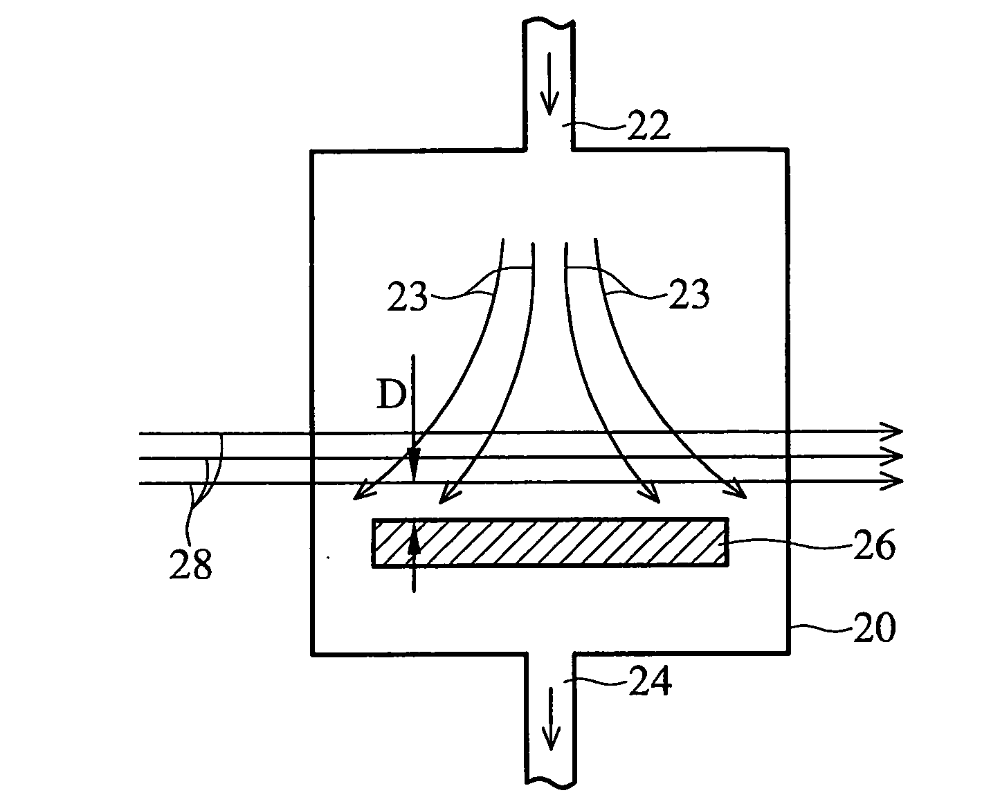
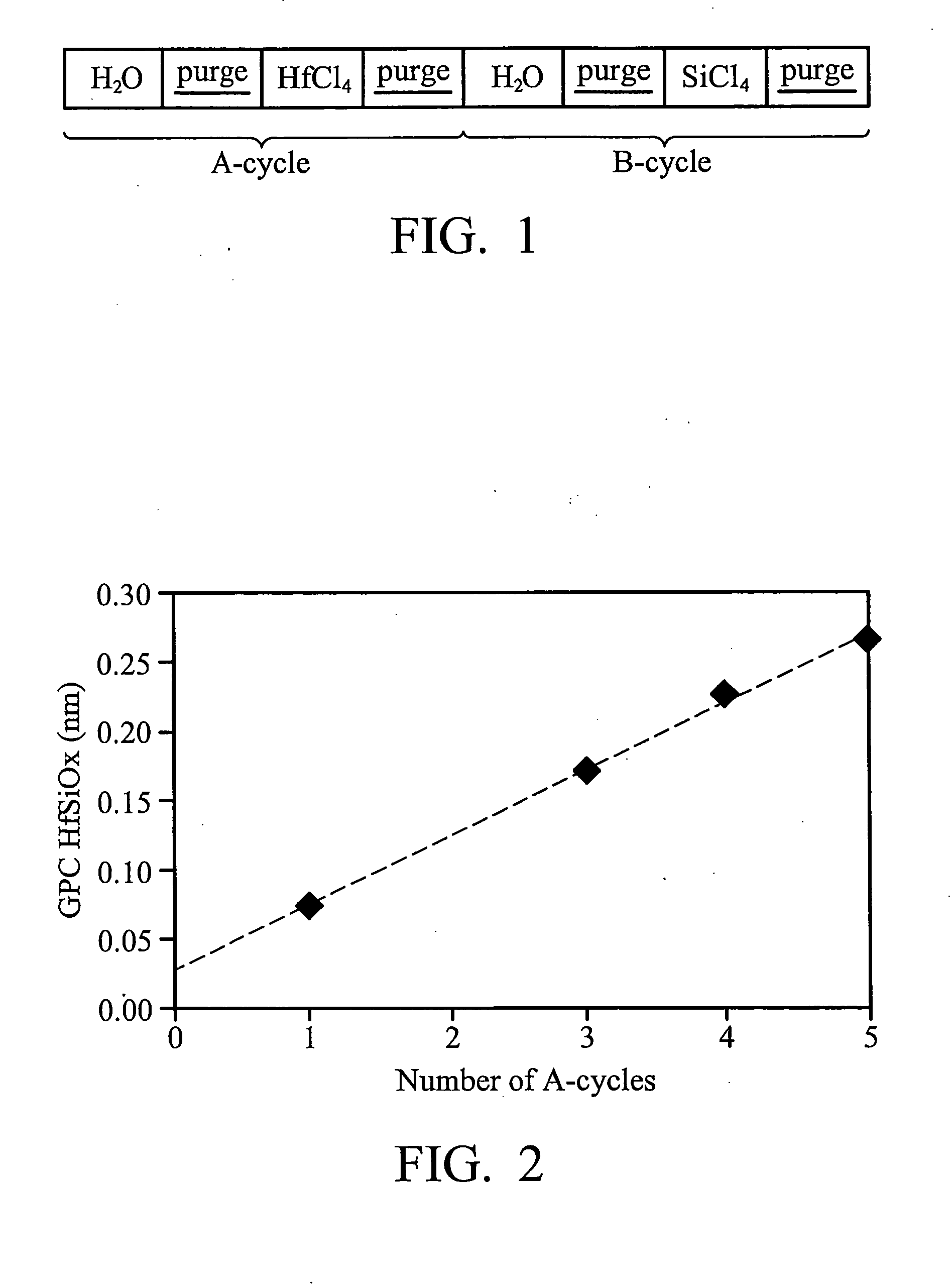
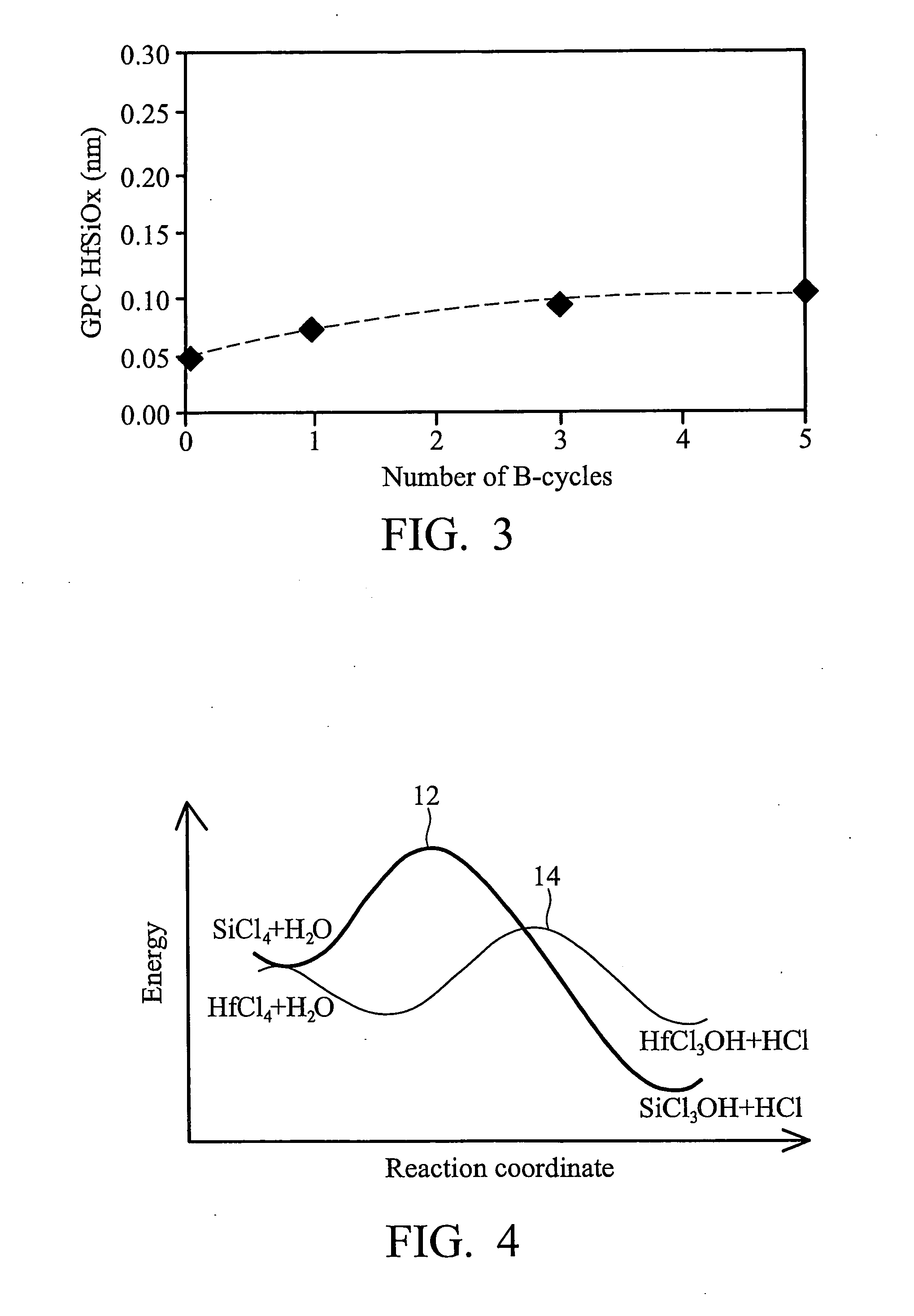
[0018]In a typical ALD process, many deposition cycles are performed. In each of the cycles, chemical reactions occur, and a thin layer is deposited. FIG. 1 illustrates exemplary cycles for forming an HfSiOx / HfO2 ...


PUM

PropertyMeasurementUnit
Distanceaaaaaaaaaa
Energyaaaaaaaaaa
Semiconductor propertiesaaaaaaaaaa

Abstract

A chemical vapor deposition (CVD) method includes placing a semiconductor wafer into a reaction chamber; introducing a precursor into the reaction chamber; activating the precursor to a high-energy state using a non-direct plasma energy source; and reacting the precursor to form a film on the semiconductor wafer.

Description

TECHNICAL FIELD[0001]This invention relates generally to integrated circuit manufacturing processes, and more particularly to chemical vapor deposition processes.BACKGROUND[0002]Chemical vapor deposition (CVD) is widely used in the semiconductor industry for manufacturing integrated circuits. There are a variety of CVD methods, such as atomic layer deposition (ALD), metal organic CVD (MOCVD), plasma enhanced CVD (PECVD), and the like. Although these methods may be based on different mechanisms, they all utilize chemical reactions, wherein gaseous reactants are introduced into reaction chambers, in which the chemical reaction occurs and products of the chemical reactions are deposited.[0003]With the increasing down-scaling of integrated circuits, devices are becoming increasingly smaller, and accordingly, the components are decreasing in size in each of the devices. For example, the thicknesses of gate dielectrics of transistors will be scaled down by about two angstroms in next gene...

Claims


Application Information

Patent Timeline
IPC IPC(8): H01L21/469H01L21/4763
CPCC23C16/40C23C16/452C23C16/45531H01L21/31645H01L21/3141H01L21/31604C23C16/45542H01L21/0228H01L21/02277H01L21/02148H01L21/02181
Inventor YU, CHEN-HUAYAO, LIANG-GI
Owner TAIWAN SEMICON MFG CO LTD
Why Eureka
Try Eureka