Nitride Semiconductor Light Emitting Device

Inactive Publication Date: 2009-05-21
ROHM CO LTD
View PDF3 Cites 20 Cited by
  • Summary
  • Abstract
  • Description
  • Claims
  • Application Information

AI Technical Summary

Benefits of technology

[0014]According to the present invention, since a light reflecting layer is formed with a multilayered film directly on a surface of the SiC substrate, film quality of nitride semiconductor layers laminated thereon is improved and even light traveling to the substrate side among light emitted in a light emitting layer becomes easy to be radiated from a surface side by being reflected by the light reflecting layer. As described above, the SiC substrate and nitride semiconductor are not matched with each other in a lattice constant or the like, and even if a buffer layer is interposed, the buffer layer can not always achieve a function of the buffer layer sufficiently because a mixed crystal ratio of Al can not be raised so high in order to keep conductivity of the buffer layer. However, since carrier concentration can be raised easily, and layers having a different lattice constant or the like can be laminated easily by making a buffer layer with a multilayer structure, a layer having a lattice constant near to that of the SiC substrate can be grown by raising the mixed crystal ratio of Al, and the film quality of nitride semiconductor layers grown thereon can be improved. In addition, the light traveling to the substrate side can be reflected by laminating the multilayered film with a t

Problems solved by technology

However, perfect lattice matching with the nitride semiconductor layer can not be achieved even if the SiC substrate is used, then, there is a problem such that light emitting efficiency decreases when crystallinity of the nitride semiconductor layer laminated thereon is poor.
However, the AlN makes an insulating layer and can not be conductive, and carrier concentration can not be enhanced with increasing Al concentration even in AlGaN based compound.
Then, when an electrode of one side is formed on a back surface of the SiC substrate, it becomes necessary to increase carrier concentration of the buffer layer sufficiently from the view point of the carrier concentration, so a limitation of increasing the mixed crystal ratio of Al is approximately 0.2.
Therefore, the lattice mismatc

Method used


Image

  • Nitride Semiconductor Light Emitting Device
  • Nitride Semiconductor Light Emitting Device
  • Nitride Semiconductor Light Emitting Device

Examples


Embodiment Construction

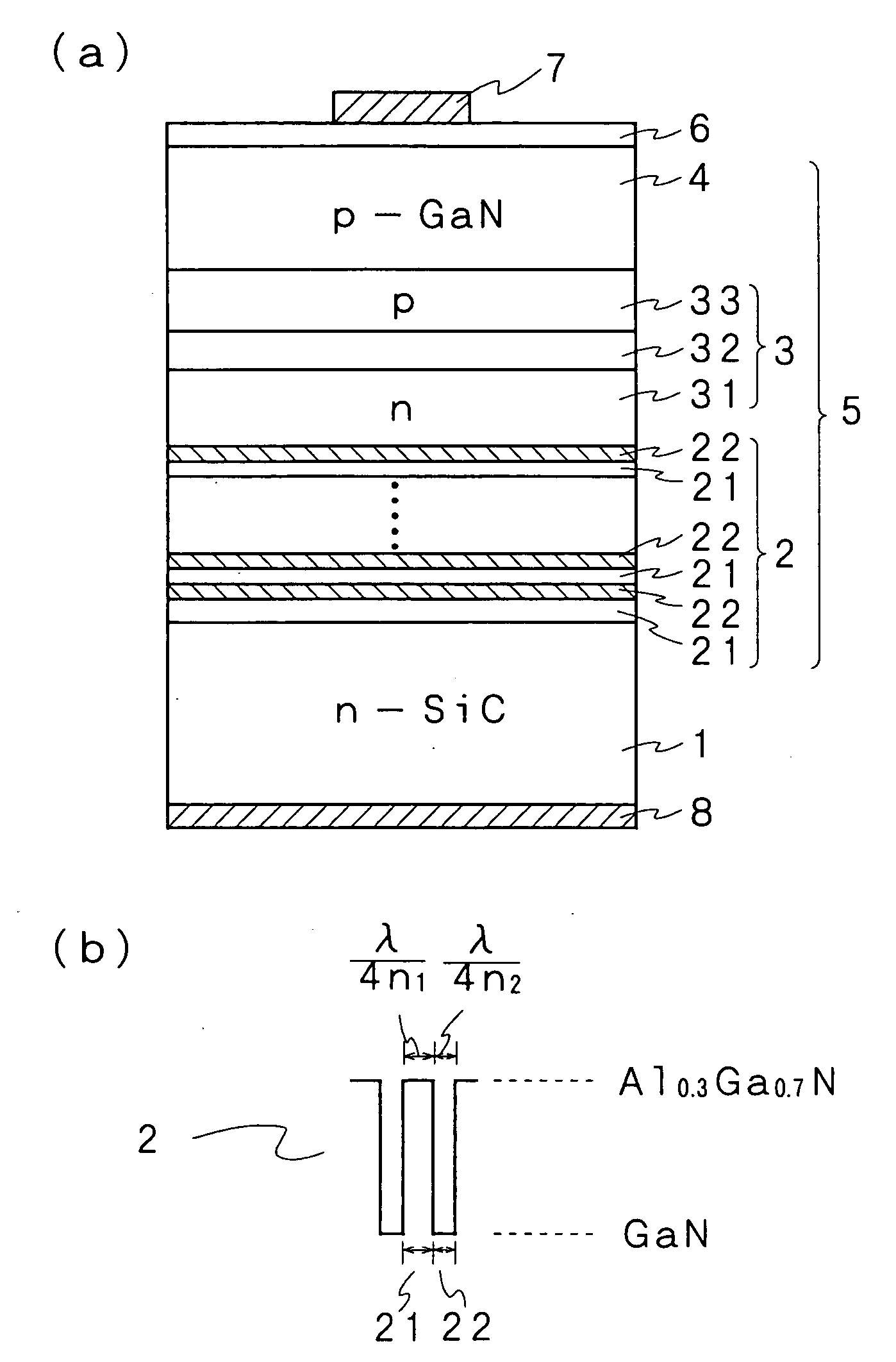
[0031]An explanation will be given below of a nitride semiconductor light emitting device according to the present invention in reference to the drawings. As an explanatory cross-sectional view of an embodiment and a figure of an energy band figure of the light reflecting layer are shown in FIG. 1, the nitride semiconductor light emitting device according to the present invention is formed such that a light reflecting layer 2 which is formed by laminating low refractive index layers 21 and high refractive index layers 22 having different refractive indices alternately is directly provided on a SiC substrate 1, and a semiconductor lamination portion 5 which is formed by laminating nitride semiconductor layers so as to form at least a light emitting layer forming portion 3 is provided on the light reflecting layer 2. And an upper electrode 7 is provided on an upper surface side of the semiconductor lamination portion 5, and a lower electrode 8 is provided on a back surface of the SiC ...


PUM


Abstract

There is provided a nitride semiconductor light emitting device capable of inhibiting output deterioration of light emission caused by quality deterioration of a nitride semiconductor layer due to lattice-mismatching between a substrate and the nitride semiconductor layer, and utilizing light traveling to the substrate efficiently, while forming a light emitting device of a vertical type which has one electrode on a back surface of the substrate by using the substrate made of SiC. A light reflecting layer (2) which is formed by laminating low refractive index layers (21) and high refractive index layers (22) having different refractive indices alternately is directly provided on the SiC substrate (1), and a semiconductor lamination portion (5) which is formed by laminating nitride semiconductor layers so as to form at least a light emitting layer forming portion (3) is provided on the light reflecting layer (2). An upper electrode (7) is provided on an upper surface side of the semiconductor lamination portion (5), and a lower electrode (8) is provided on a back surface of the SiC substrate (1).

Description

FIELD OF THE INVENTION[0001]The present invention relates to a semiconductor light emitting device using nitride semiconductor. More particularly, the present invention relates to a nitride semiconductor light emitting device using a substrate made of SiC, capable of taking out light emitted in a light emitting layer forming portion efficiently while providing one electrode on a back surface of the substrate, and improving external quantum efficiency.BACKGROUND OF THE INVENTION[0002]A conventional semiconductor light emitting device using nitride semiconductor is formed by growing a nitride semiconductor lamination portion including a buffer layer and a light emitting layer forming portion, for example, on a sapphire substrate, exposing a conductivity type layer of a lower layer side of the semiconductor lamination portion by etching a part of the semiconductor lamination portion, and providing a lower electrode on a surface of the exposed conductivity type layer of the lower layer ...

Claims


Application Information

Patent Timeline
IPC IPC(8): H01L33/00H01L33/06H01L33/10H01L33/32H01L33/42
CPCH01L33/10H01S5/32341H01S5/187H01L33/32
Inventor TANAKA, HARUOSONOBE, MASAYUKI
Owner ROHM CO LTD
Why Eureka
Try Eureka