Manufacturing method of semiconductor device

Active Publication Date: 2007-02-13
FUJITSU SEMICON LTD
View PDF3 Cites 32 Cited by
  • Summary
  • Abstract
  • Description
  • Claims
  • Application Information

AI Technical Summary

Benefits of technology

[0022]It is an object of the present invention to provide a manufacturing method a semiconductor device capable of improving the characteristic of a dielectric film formed on a capacitor lower electrode by improving a film quality of a conductive film constituting the capacitor lower electrode.

Problems solved by technology

However, according to such Ti-film forming method, it may be considered that since H2O is always present in the surrounding atmosphere of the Ti film during the sputter, it is difficult to get a pure film quality.
However, since H2O remains in an inside of Ti-film forming chamber for a while even after shutting of the introduction of H2O, it is impossible to perfectly avoid the mixture of H2O into an upper portion of the Ti film.
Therefore, when the number of sheets of the processed wafer on which Ti is formed is increased, it is uncertain whether or not the Ti film with the same film quality can be supplied.
Thus, there arises possibility that the stable plasma cannot be maintained in the chamber.
Since the O—H bond itself is unstable and also presence of one Si—OH group to ten Si—O groups is stable on the surface, it is difficult to increase the density of hydrogen termination on the surface of the insulating film.

Method used


Image

  • Manufacturing method of semiconductor device
  • Manufacturing method of semiconductor device
  • Manufacturing method of semiconductor device

Examples


first embodiment

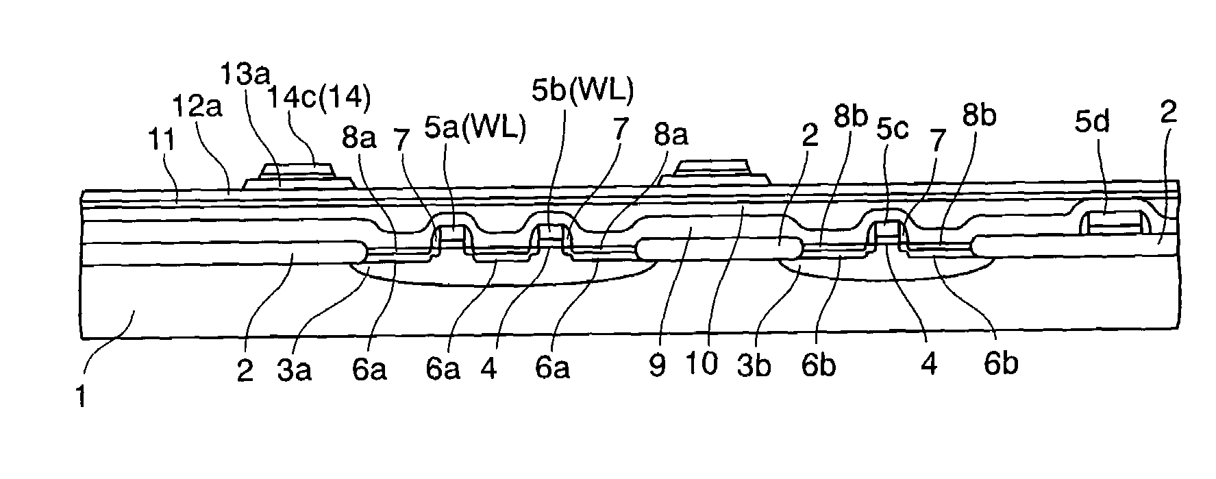
[0053]FIGS. 1A to 1R are sectional views showing steps of manufacturing a semiconductor device according to a first embodiment of the present invention.

[0054]Steps required until a structure shown in FIG. 1A is formed will be explained hereunder.

[0055]First, as shown in FIG. 1A, an element isolation insulating film 2 is formed on a surface of an n-type or p-type silicon (semiconductor) substrate 1 by the LOCOS (Local Oxidation of Silicon) method. As the element isolation insulating film 2, the STI (Shallow Trench Isolation) structure may be employed in place of the structure formed by the LOCOS method.

[0056]After such element isolation insulating film 2 is formed, a p-well 3a and an n-well 3b are formed by introducing the p-type impurity and the n-type impurity selectively into predetermined active regions (transistor forming regions) in a memory cell region A and a peripheral circuit region B of the silicon substrate 1.

[0057]In this case, a p-well (not shown) as well as the n-well ...

second embodiment

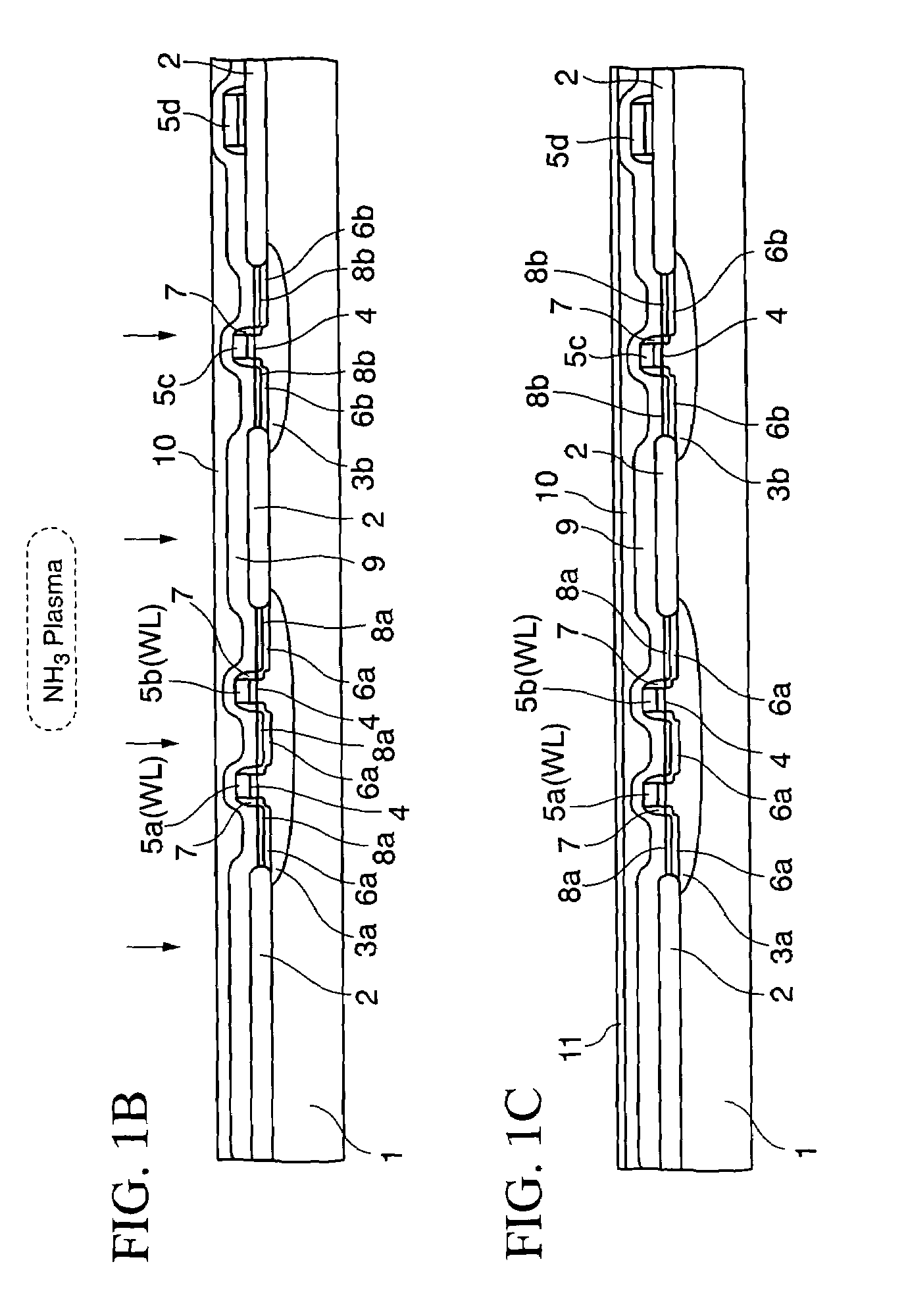
[0215]In the first embodiment, the conditions applied to form the ferroelectric film by the sputter is explained as above. In the second embodiment, the conditions applied to form the ferroelectric film by the MOCVD method will be explained hereunder.

[0216]First, as shown in FIG. 1A, the upper surface of the first interlayer insulating film 10 is planarized by the CMP. Then, as shown in FIG. 1B, the first interlayer insulating film 10 is exposed to the NH3 plasma. As the conditions for the NH3 plasma process, for example, a flow rate of the NH3 gas introduced into the chamber is set to 250 sccm, a pressure in the chamber is set to 4 Torr, a substrate temperature is set to 350° C., a power of the RF power supply supplied to the substrate is set to 100 W, a power of the RF power supply supplied to the plasma generating area is set to 55 W, a distance between the electrode—the first interlayer insulating film is set to 300 mils, and a plasma irradiating time is set to 1 minute.

[0217]Th...

third embodiment

[0248]In the first and second embodiments, the FeRAM having the planar capacitor of the structure in which the upper electrode and the lower electrode are extended electrically from the top is explained as above. In the third embodiment, the FeRAM memory cell having the stacked capacitor of the structure in which the lower electrode is extended electrically from the bottom will be explained hereunder.

[0249]FIGS. 25A to 25I are sectional views showing steps of manufacturing a semiconductor device according to a third embodiment of the present invention.

[0250]First, steps required until a sectional structure shown in FIG. 25A is formed will be explained hereunder.

[0251]As shown in FIG. 25A, an element isolation recess is formed round a transistor forming region of an n-type or p-type silicon (semiconductor) substrate 51 by the photolithography method. Then, an element isolation insulating film 52 having the STI structure is formed by burying silicon oxide (SiO2) into the element isola...


PUM

PropertyMeasurementUnit
Temperatureaaaaaaaaaa
Pressureaaaaaaaaaa

Abstract

There are provided a step of forming an insulating film over a semiconductor substrate, a step of exciting a plasma of a gas having a molecular structure in which hydrogen and nitrogen are bonded and then irradiating the plasma onto the insulating film, a step of forming a self-orientation layer made of substance having a self-orientation characteristic on the insulating film, and a step of forming a first conductive film made of conductive substance having the self-orientation characteristic on the self-orientation layer.

Description

CROSS-REFERENCE TO RELATED APPLICATIONS[0001]This application is based upon and claims priority of Japanese Patent Application No. 2002-316894, filed on Oct. 30, 2002, the contents being incorporated herein by reference.BACKGROUND OF THE INVENTION[0002]1. Field of the Invention[0003]The present invention relates to a manufacturing method of a semiconductor device and, more particularly, to a manufacturing method of a semiconductor device having a capacitor.[0004]2. Description of the Related Art[0005]As the nonvolatile memory that can still store the information after the power supply is turned off, the flash memory and the ferroelectric memory (FeRAM) are known.[0006]The flash memory has a floating gate that is buried in a gate insulating film of the insulated-gate field effect transistor (IGFET), and stores the information by accumulating a charge indicating the stored information in the floating gate. A tunnel current that passes through the gate insulating film must be supplied ...

Claims


Application Information

Patent Timeline
IPC IPC(8): H01L21/44C23C16/40H01L21/02H01L21/314H01L21/8242H01L21/8246H01L27/06H01L27/105H01L27/108
CPCH01L21/3144H01L28/40H01L27/0629H01L21/02164H01L21/02216H01L21/02282H01L21/02271H01L21/02274H01L21/02197H01L27/105H01L21/02356H01L21/02337H01L21/0234
Inventor SASHIDA, NAOYAMATSUURA, KATSUYOSHIHORII, YOSHIMASAKURASAWA, MASAKITAKAI, KAZUAKI
Owner FUJITSU SEMICON LTD
Why Eureka
Try Eureka