Display apparatus
a technology of display apparatus and display screen, which is applied in the direction of discharge tube/lamp details, cathode-ray/electron beam tube electrical connection, discharge tube/lamp details, etc., can solve problems such as voltage distribution, and achieve the effect of preventing the resistance of the entire common electrod
- Summary
- Abstract
- Description
- Claims
- Application Information
AI Technical Summary
Benefits of technology
Problems solved by technology
Method used
Image

Examples
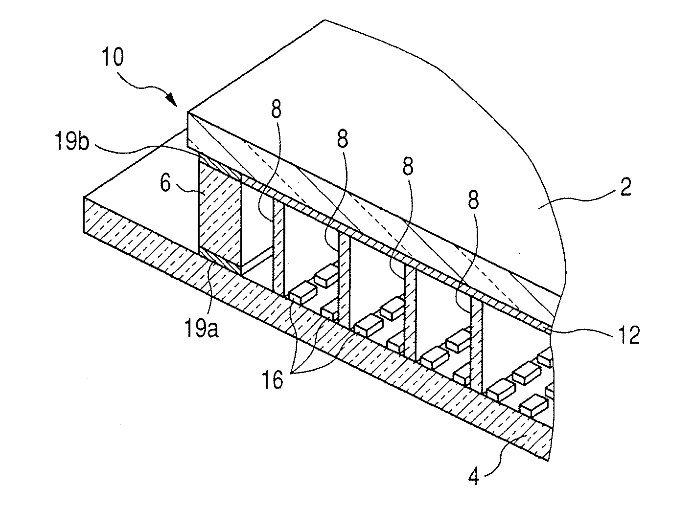
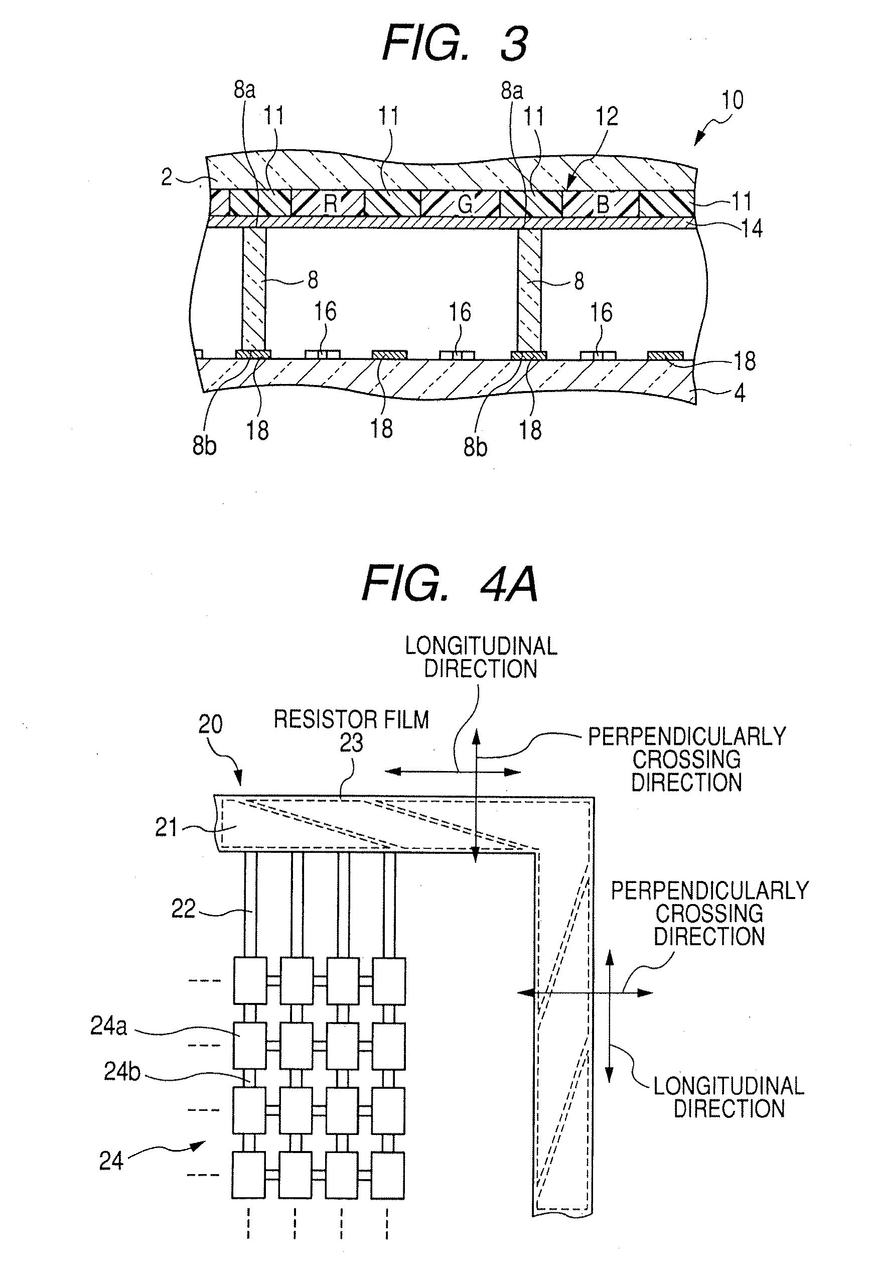
first embodiment
[0040]FIG. 4A is a schematic diagram partially and enlargedly showing the structures of a metal back and a common electrode provided in the inner surface of a front substrate in a first embodiment of the present invention.
[0041]As shown in FIG. 4A, a metal back 24 of the present embodiment is segmentalized into a plurality of rectangular island-shaped areas 24a. More specifically, for example, the rectangular island-shaped areas 24a to cover phosphor layers R, G, and B not illustrated here on a one-to-one correspondence are formed in a matrix pattern, and each segmentalized area 24a is electrically connected via a resistor member 24b.
[0042]On the other hand, a common electrode 20 is annularly provided so as to surround the periphery of the metal back 24. The common electrode 20 includes a plurality of electrode films 21 spaced-apart in its longitudinal direction, and a resistor film 23 is annularly provided superposed on the electrode films 21 so as to annularly connect the electro...
second embodiment
[0044]FIG. 5 is a schematic diagram partially and enlargedly showing the structures of a metal back and a common electrode provided in the inner surface of a front substrate in a second embodiment of the present invention.
[0045]In the present embodiment also, a common electrode 20 is annularly provided so as to surround the periphery of the metal back 24. The common electrode 20 includes a plurality of electrode films 21 spaced-apart in its longitudinal direction, and a resistor film 23 is annularly provided superposed on the electrode films 21 so as to annularly connect the electrode films 21. The resistor film 23 of the common electrode 20 is connected to the edge portion of the metal back 24 via the resistor film 22.
[0046]In the present embodiment, the portion opposed to each other of each electrode film 21 has a portion extended to the longitudinal direction of the common electrode 20 and a portion extended in the width direction of the common electrode 20 orthogonal to the long...
third embodiment
[0051]FIG. 7 is a schematic diagram partially and enlargedly showing the structures of a metal back and a common electrode provided in the inner surface of a front substrate in a third embodiment of the present invention.
[0052]In the present embodiment also, a common electrode 20 is annularly provided so as to surround the periphery of the metal back 24. The common electrode 20 includes a plurality of electrode films 21 spaced-apart in its longitudinal direction, and a resistor film 23 is annularly provided superposed on the electrode films 21 so as to annularly connect the electrode films 21. The resistor film 23 of the common electrode 20 is connected to the edge portion of the metal back 24 via the resistor film 22.
[0053]In the present embodiment, the portion opposed to each other of each electrode film 21 has a portion extended to the longitudinal direction of the common electrode 20 and a portion extended in the width direction of the common electrode 20, and has a comb teeth e...
PUM
 Abstract
Description
Claims
Application Information
 - R&D
- Intellectual Property
- Life Sciences
- Materials
- Tech Scout
- Unparalleled Data Quality
- Higher Quality Content
- 60% Fewer Hallucinations
Browse by: Latest US Patents, China's latest patents, Technical Efficacy Thesaurus, Application Domain, Technology Topic, Popular Technical Reports.
© 2025 PatSnap. All rights reserved.Legal|Privacy policy|Modern Slavery Act Transparency Statement|Sitemap|About US| Contact US: help@patsnap.com