Substrate processing apparatus

a processing apparatus and substrate technology, applied in the direction of chemistry apparatus and processes, cleaning using liquids, coatings, etc., can solve the problems of complicated routing of tubes described above and the need for extra parts of tubes, and achieve the effect of reducing the number of parts

Active Publication Date: 2008-07-31
TOKYO ELECTRON LTD
View PDF33 Cites 6 Cited by
  • Summary
  • Abstract
  • Description
  • Claims
  • Application Information

AI Technical Summary

Benefits of technology

[0013]The present invention provides a substrate pro...

Problems solved by technology

Since the deposit film may cause problems in the semiconductor device, such as conduction failure, the deposit film must be removed.
However, in and around the upper lid of the chamber, the introduction tube described above is routed in a comp...

Method used


Image

  • Substrate processing apparatus
  • Substrate processing apparatus
  • Substrate processing apparatus

Examples


first embodiment

[0028]First, a description will be made of a substrate processing system including a substrate processing apparatus according to the present invention.

[0029]FIG. 1 is a plan view schematically showing the configuration of the substrate processing system including the substrate processing apparatus according to present embodiment.

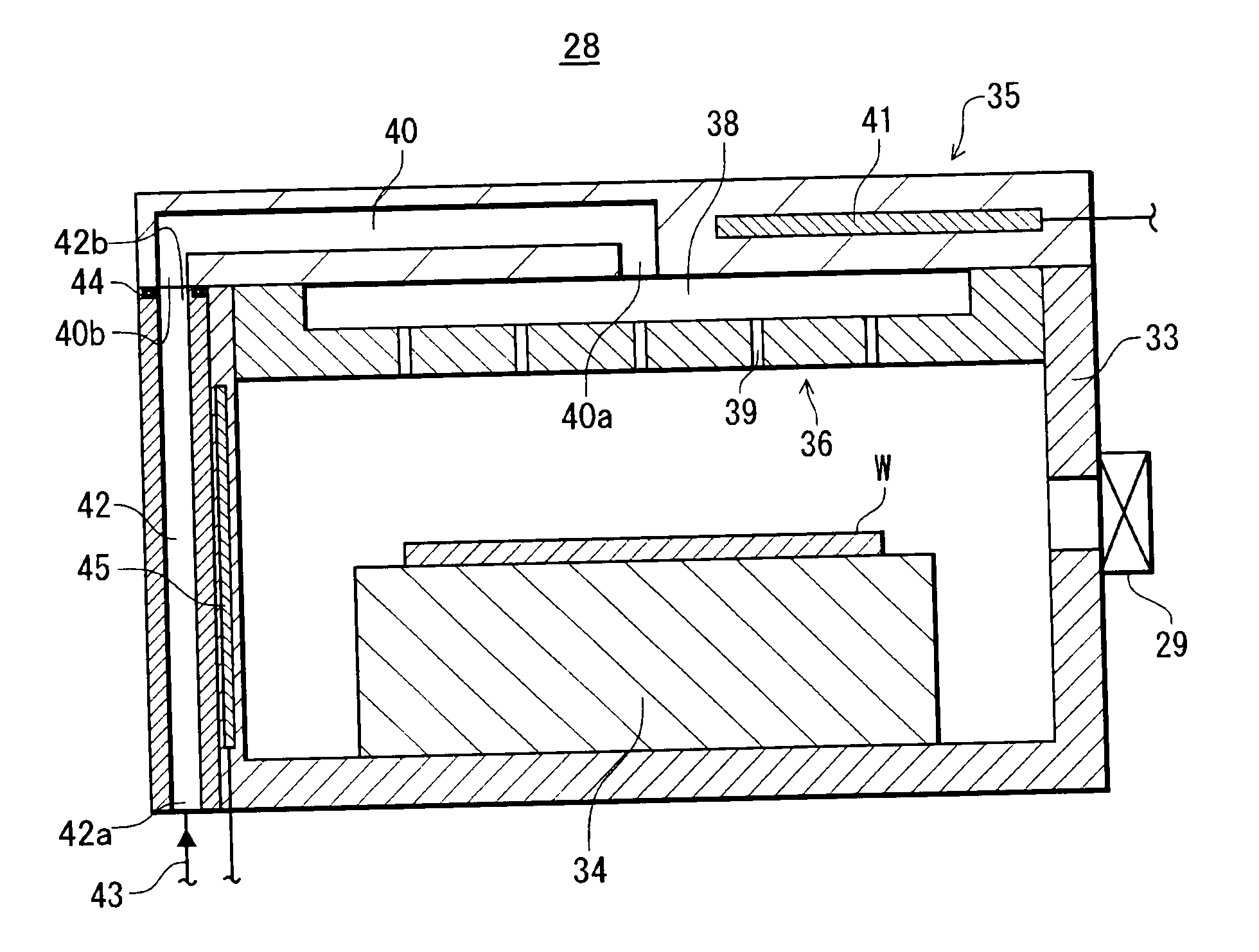
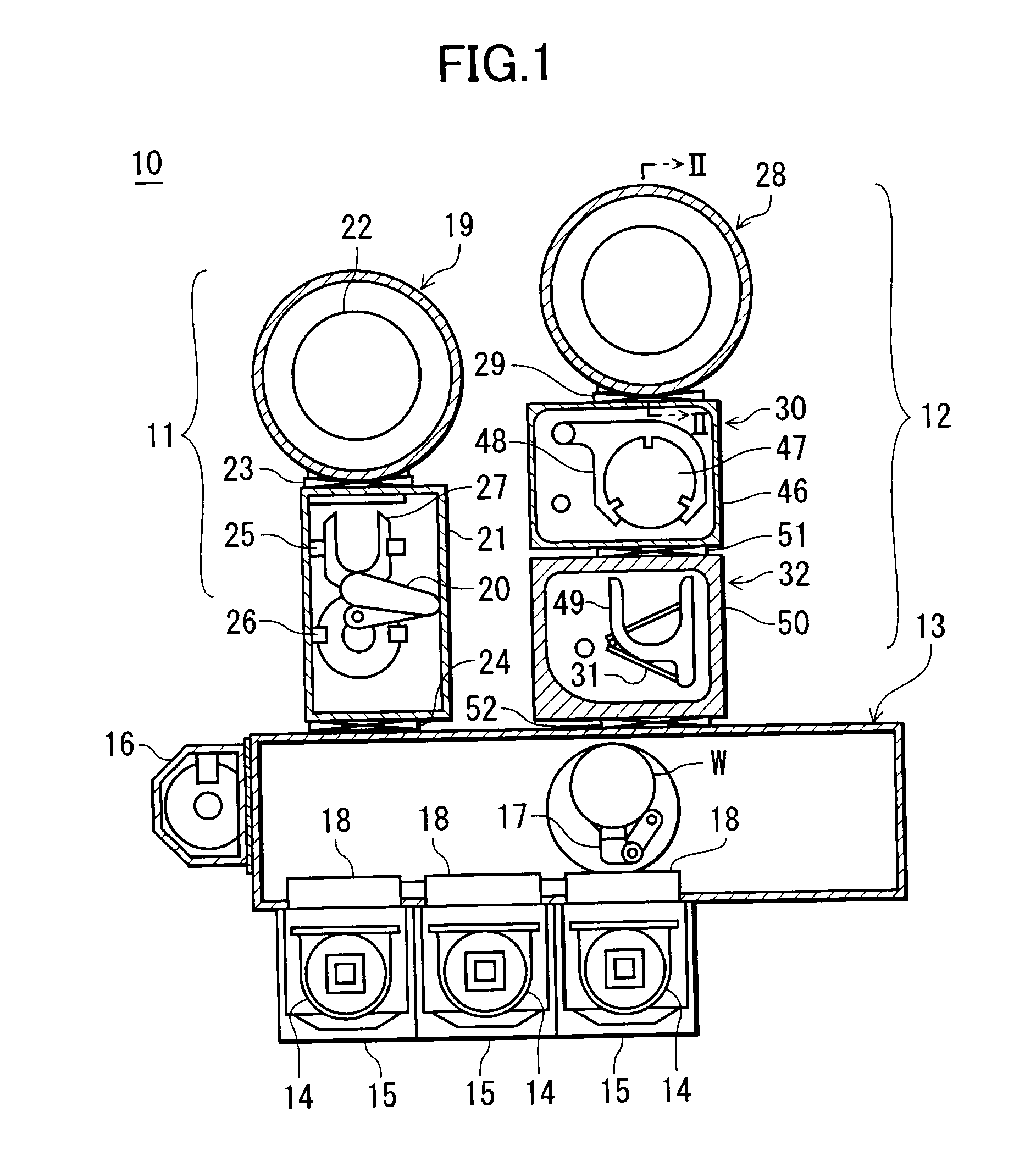
[0030]In FIG. 1, the substrate processing system 10 includes a first process ship 11 that carries out plasma processing on a wafer (substrate) for semiconductor devices (hereinafter simply referred to as “wafer”) W, and a second process ship 12 disposed parallel to the first process ship 11 and configured to carry out chemical reaction processing and heating processing, which will be described later, on the wafer W. The substrate processing system 10 further includes a loader module 13, which serves as a box-shaped common transfer chamber to which the first and second process ships 11 and 12 are connected.

[0031]In addition to the first and second process shi...

second embodiment

[0056]Next, a description will be made of a substrate processing system including a substrate processing apparatus according to the present invention.

[0057]The present embodiment is basically the same as the first embodiment described above in terms of the configuration and actions, but only differs from the first embodiment in terms of the configuration of the second process module. Accordingly, no description will be made of the similar configuration and only the configuration and actions different from those in the first embodiment will be described below.

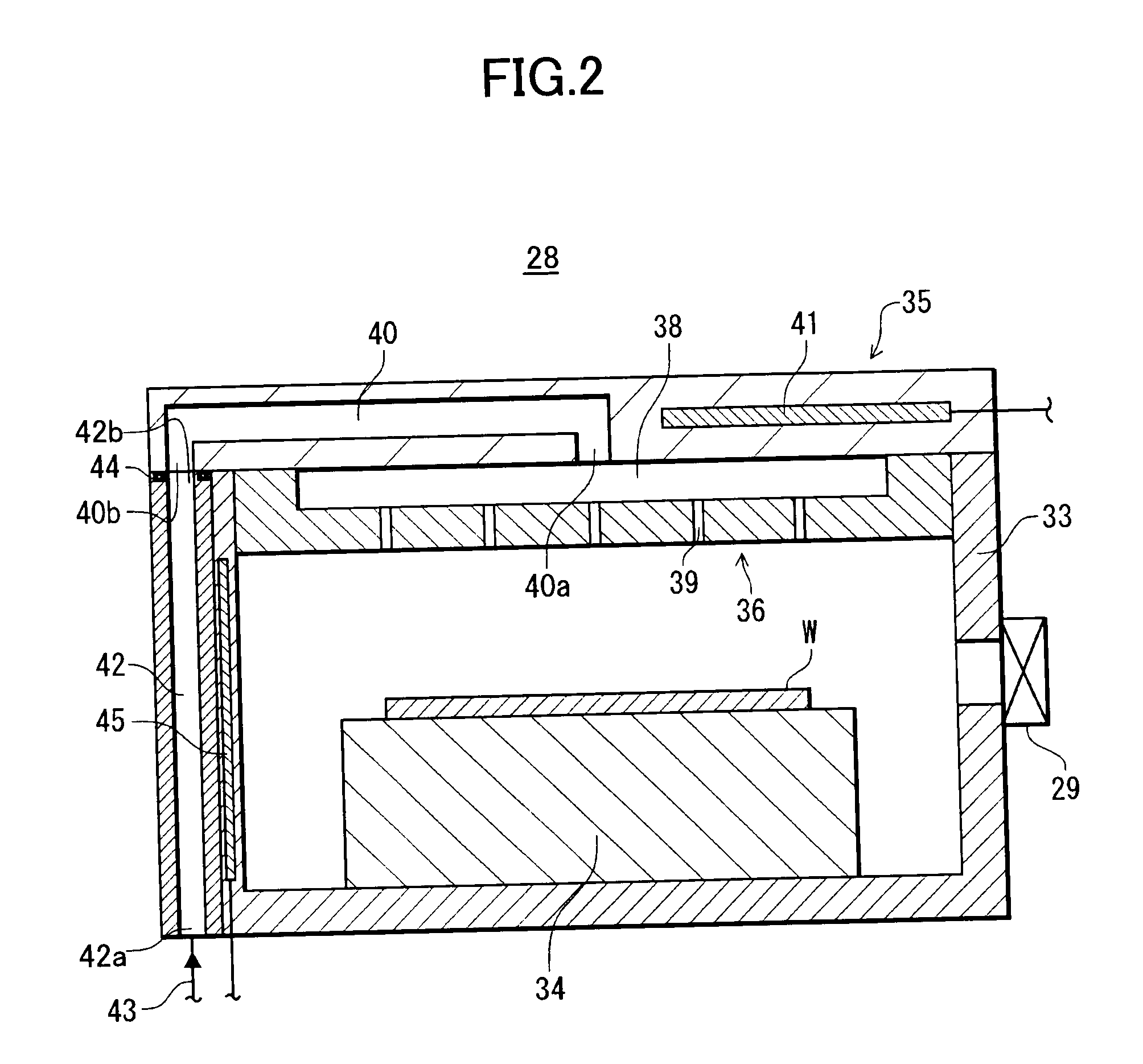
[0058]FIG. 4 is a cross-sectional view of the second process module in the present embodiment.

[0059]In FIG. 4, a second process module 53 has a cylindrical processing vessel 55 to which a gas introduction tube 54 is attached. The gas introduction tube 54 introduces hydrogen fluoride gas from a hydrogen fluoride gas source (not shown). One end 54a of the gas introduction tube 54 is connected to the gas introduction tube 43 throug...


PUM

PropertyMeasurementUnit
Temperatureaaaaaaaaaa

Abstract

A substrate processing apparatus that can reduce the number of parts. A first gas introduction hole through which the hydrogen fluoride gas is introduced into a GDP is formed in an upper lid. A second gas introduction hole through which hydrogen fluoride gas is introduced from a hydrogen fluoride gas source is formed in a processing vessel. When the upper lid engages the upper portion of the processing vessel, one end of the first gas introduction hole is joined with one end of the second gas introduction hole to form an introduction path through which the hydrogen fluoride gas is introduced into a chamber.

Description

BACKGROUND OF THE INVENTION[0001]1. Field of the Invention[0002]The present invention relates to a substrate processing apparatus, and particularly to a substrate processing apparatus having an upper lid that engages a processing vessel to define a substrate processing chamber.[0003]2. Description of the Related Art[0004]In a semiconductor device manufacturing method for manufacturing a semiconductor device from a silicon wafer (hereinafter simply referred to as “wafer”), the following steps are repeatedly carried out in a sequential manner: a film formation step of forming a conductive film or an insulating film on the surface of the wafer using CVD (Chemical Vapor Deposition) or the like, a lithography step of forming a photoresist layer having a desired pattern on the formed conductive film or insulating film, and an etching step of using the photoresist layer as a mask to shape the conductive film into a gate electrode or form a wiring groove or a contact hole in the insulating ...

Claims


Application Information

Patent Timeline
IPC IPC(8): B05C5/00
CPCC23C16/4401C23C16/54C23C16/4411H01L21/205
Inventor HAYASHI, DAISUKE
Owner TOKYO ELECTRON LTD
Why Eureka
Try Eureka