Ceramic LED package

a technology of led packaging and ceramics, applied in the direction of circuit optical details, electrical apparatus construction details, printed circuit aspects, etc., can solve the problems of accelerated aging, high device temperature, and harm to semiconductors

Inactive Publication Date: 2008-07-31
SEMILEDS OPTOELECTRONICS CO LTD
View PDF10 Cites 115 Cited by
  • Summary
  • Abstract
  • Description
  • Claims
  • Application Information

AI Technical Summary

Benefits of technology

[0009]One embodiment of the present invention provides a packaged light-emitting diode (LED) device. The packaged LED device generally includes a ceramic substrate having a top cavity and a bottom cavity; one or more LED dies coupled to a plurality of connection pads, the connection pads being disposed within the top cavity of the ceramic substrate and coupled by electrical vias to terminals for external connection; and a metallic insert disposed within the bottom cavity of the ceramic substrate for conducting heat away from the LED dies.
[0010]Another embodiment of the present invention provides a package for at least partially encasing one or more LED dies. The package generally includes a ceramic substrate having a cavity underneath an area designated for the LED dies; and a thermally conductive insert disposed within the cavity for conducting heat away from the LED dies.
[0011]Yet another embodiment of the present invention provides a packaged LED device. The packaged LED device generally includes a ceramic substrate having an upper portion and a lower portion; a plurality of connection pads disposed within a cavity of the ceramic substrate's upper portion and coupled by electrical vias to terminals for external connection; and one or more LED dies coupled to the plurality of connection pads and disposed within the cavity, wherein a plurality of thermal vias comprised of a composite are provided in the ceramic substrate's lower portion for conducting heat away from the LED dies.
[0012]Yet another embodiment of the present invention provides a ceramic substrate for at least partially encasing one or more LED dies. The ceramic substrate generally includes an upper portion having a cavity for disposing the LED dies therein and a lower portion providing a plurality of thermal vias comprised of a composite for conducting heat away from the LED dies.

Problems solved by technology

When LEDs are driven with high currents, high device temperatures may occur because of insufficient heat transfer from the p-n junction of the semiconductor die to the ambient environment.
Such high temperatures may harm the semiconductor and lead to such degradations as accelerated aging, separation of the LED die from the lead frame, and breakage of bond wires.
In addition to the aforementioned problems, the optical properties of the LED vary with temperature, as well.
The problem with this design is that the majority of the lead frame 4a, 4b is situated within the ceramic package 1,2, which acts as a thermal insulator, and the main path for heat dissipation out of the device is limited by the size of the leads.
Even designs that have added to the size or number of leads in an effort to promote heat transfer still possess an inherent bottleneck for heat dissipation, as the leads are still sandwiched in the thermally insulative ceramic package.
However, the insulative properties of the growth substrate limit the potential heat dissipation.
Furthermore, if the LED dies are vertical light-emitting diode (VLED) dies having LED stacks disposed above a metal substrate, the electrically conductive thermal vias make electrical contact with the metal substrate, thereby decreasing the flexibility of the circuit layout

Method used


Image

  • Ceramic LED package
  • Ceramic LED package
  • Ceramic LED package

Examples


Embodiment Construction

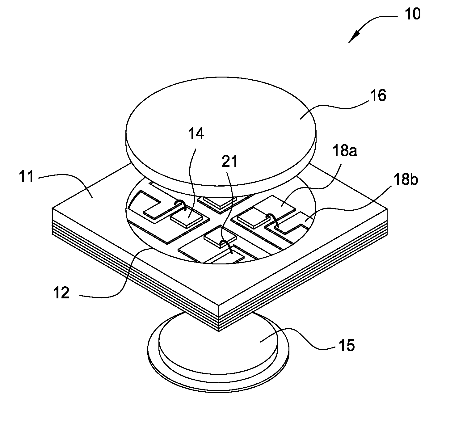
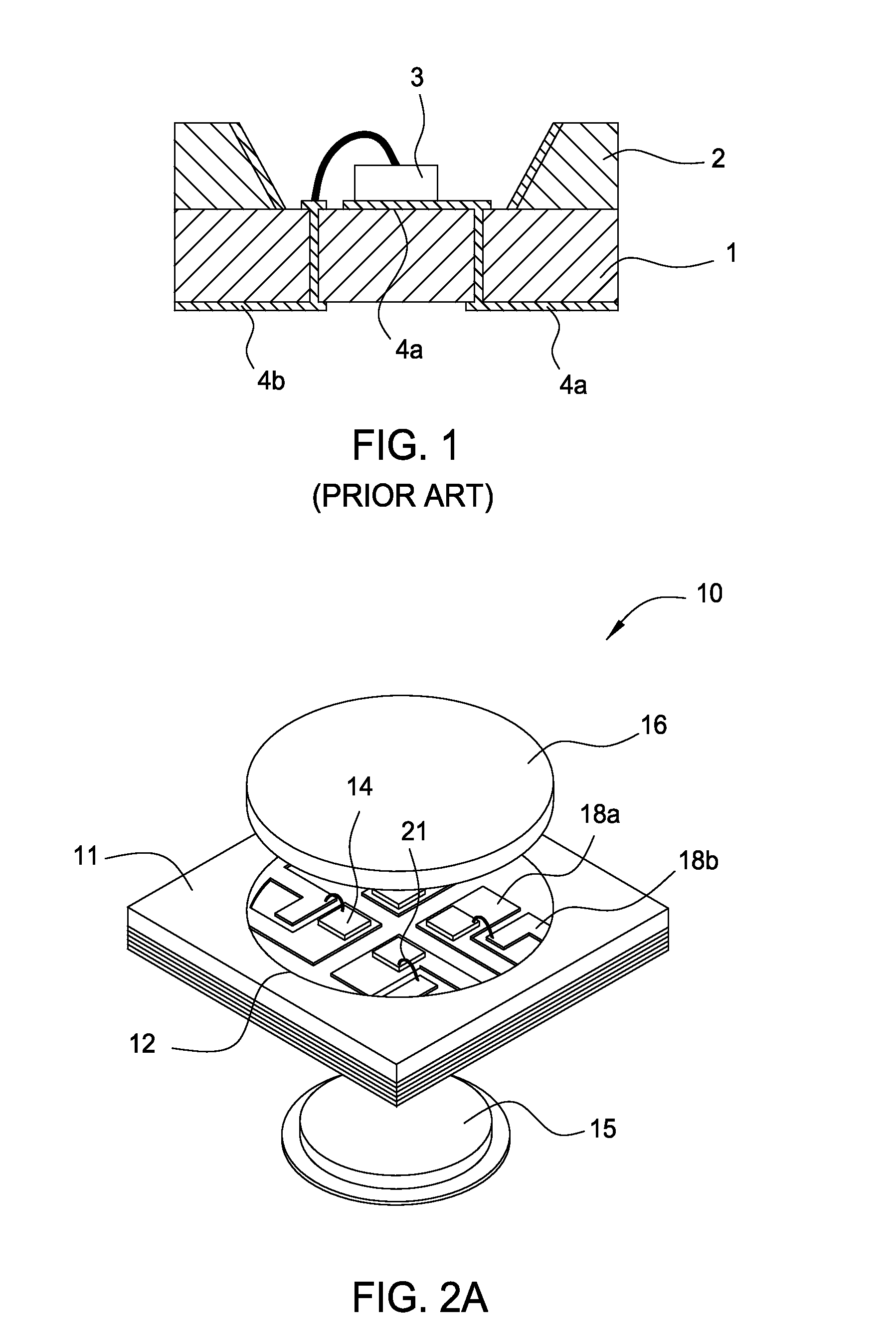
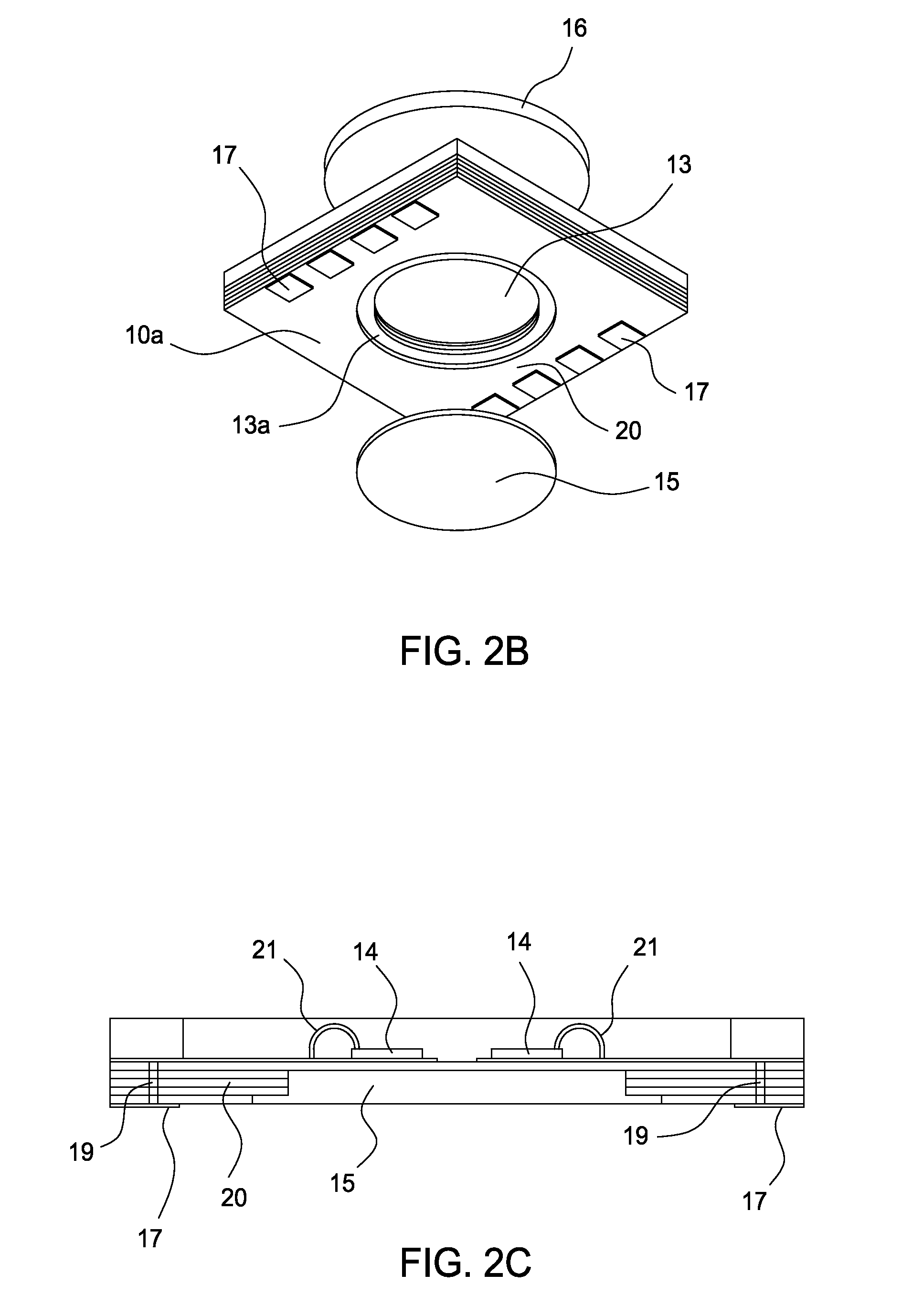
[0020]Embodiments of the present invention provide light-emitting diode (LED) packages with improved heat transfer paths for LED dies encased therein when compared to conventional LED packages. For some embodiments, the LED package includes a ceramic substrate having a top cavity with one or more LED dies disposed within and having a bottom cavity for receiving a metallic insert to dissipate heat away from the LED dies. For other embodiments, an LED package is provided that includes a ceramic substrate having a heat spreader coupled to thermal vias filled with a highly thermally conductive composite.

An Exemplary LED Package

[0021]FIGS. 2A-B illustrate various components of an LED package 10 when viewed from two different perspectives according to one embodiment of the invention. The LED package 10 may comprise a multilayered ceramic substrate 11 having a top cavity 12 and a bottom cavity 13. Within the top cavity 12, one or more LED dies 14 may be disposed on connection pads 18a. Dep...


PUM

PropertyMeasurementUnit
thermal conductivityaaaaaaaaaa
metallicaaaaaaaaaa
temperatureaaaaaaaaaa

Abstract

Light-emitting diode (LED) packages with improved heat transfer paths for LED dies encased therein when compared to conventional LED packages are provided. For some embodiments, the LED package includes a ceramic substrate having a top cavity with one or more LED dies disposed within and having a bottom cavity for receiving a metallic insert to dissipate heat away from the LED dies. For other embodiments, an LED package is provided that includes a ceramic substrate having a heat spreader coupled to thermal vias filled with a highly thermally conductive composite.

Description

BACKGROUND OF THE INVENTION[0001]1. Field of the Invention[0002]Embodiments of the present invention generally relate to the field of light-emitting diode (LED) technology and, more particularly, to LED packaging.[0003]2. Description of the Related Art[0004]Heat transfer management is a concern for designers of light-emitting diodes (LEDs). When LEDs are driven with high currents, high device temperatures may occur because of insufficient heat transfer from the p-n junction of the semiconductor die to the ambient environment. Such high temperatures may harm the semiconductor and lead to such degradations as accelerated aging, separation of the LED die from the lead frame, and breakage of bond wires.[0005]In addition to the aforementioned problems, the optical properties of the LED vary with temperature, as well. As an example, the light output of an LED typically decreases with increased junction temperature. Also, the emitted wavelength can change with temperature due to a change i...

Claims


Application Information

Patent Timeline
Patent Type & Authority Applications(United States)
IPC IPC(8): H01L33/00H05K7/20H01L33/48H01L33/62H01L33/64
CPCH01L25/0753H01L33/486H01L33/62H01L33/641H01L2224/48091H01L2224/48227H01L2924/01322H01L2924/01046H01L2924/01079H01L2924/09701H01L2924/01004H01L2924/01019H01L2924/00014H05K1/0204H05K1/0206H05K1/0274H05K1/0306H05K3/284H05K2201/0224H05K2201/026H05K2201/0272H05K2201/0323H05K2201/10106H05K2201/10113
Inventor CHENG, CHING-TAI
Owner SEMILEDS OPTOELECTRONICS CO LTD
Why Eureka
Try Eureka