Semiconductor device and method of producing the same

Inactive Publication Date: 2008-07-31
FUJITSU SEMICON LTD
View PDF11 Cites 5 Cited by
  • Summary
  • Abstract
  • Description
  • Claims
  • Application Information

AI Technical Summary

Benefits of technology

[0009]According to the present invention, there is provided a semiconductor device having a conductive film formed over a substrate, an insulating film formed over the conductive film, and having a hole on the conductive film, and a conductive plug formed in the hole including a barrier metal film and a conduc

Problems solved by technology

However, when tungsten diffuses in an interlayer insulating film disposed on the peripheries of the tungsten plugs, a problem of an increase in the leakage current at the boundary between the tungsten plugs and the interlayer insulating film occurs.
As a result, the contact resistance becomes unstable.
However, the formation of such a barrier metal film causes a problem of an increase in the contact resistance between an underlayer, such as a metal silicide layer, and the conductive plugs.
As a result, circuits formed on a semiconductor substrate do not function as they are designed to, resulting in a decrease in the yield of the semiconductor device.

Method used


Image

  • Semiconductor device and method of producing the same
  • Semiconductor device and method of producing the same
  • Semiconductor device and method of producing the same

Examples


Embodiment Construction

[0029]An embodiment of the present invention will now be described in detail with reference to the attached drawings.

[0030]FIGS. 1A to 14 are cross-sectional views showing steps of a method of producing a semiconductor device according to the embodiment of the present invention.

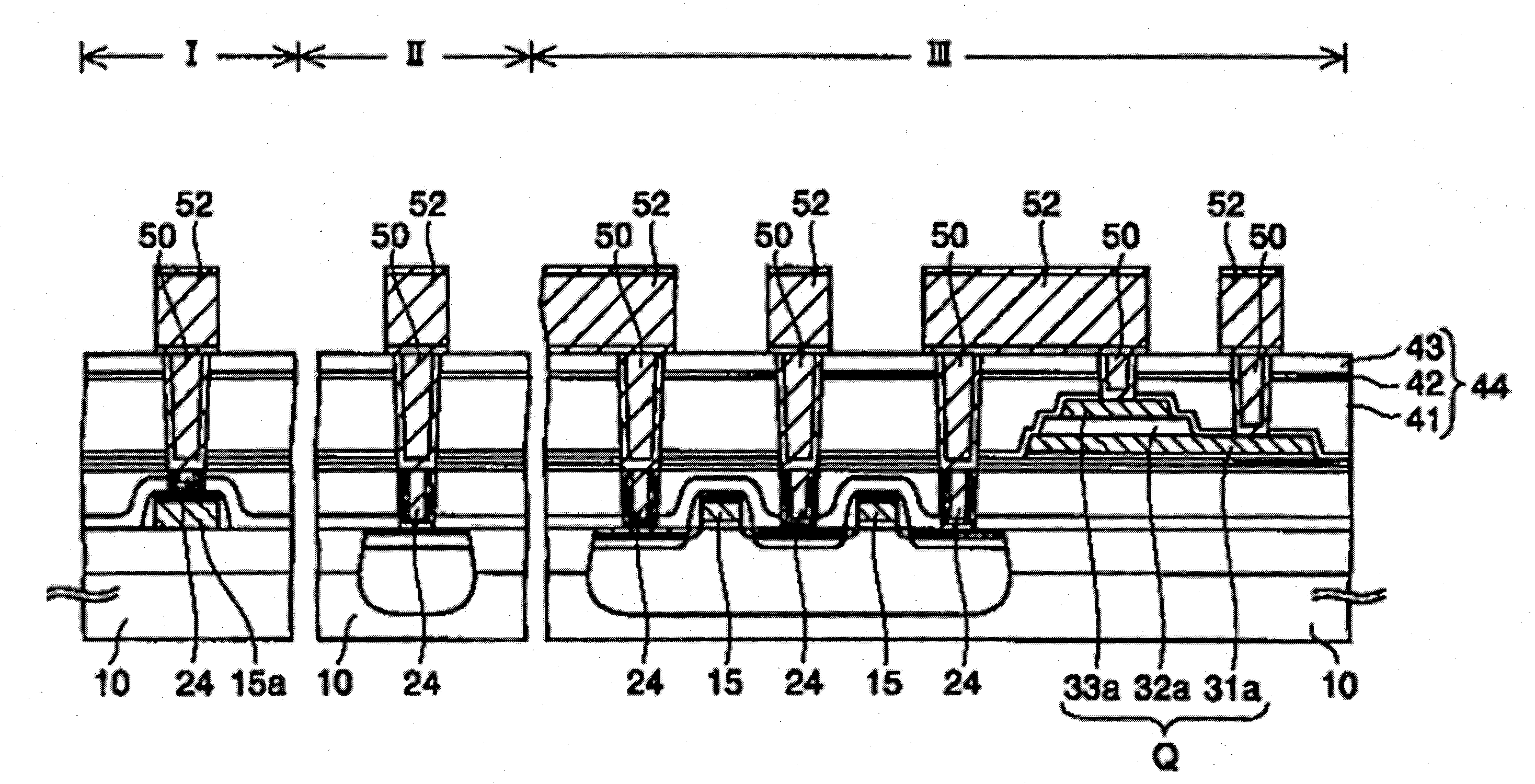
[0031]This semiconductor device is a planar ferroelectric random access memory (FeRAM) including a gate contact region I, a well contact region II, and a capacitor-forming region III. This semiconductor device is produced as follows.

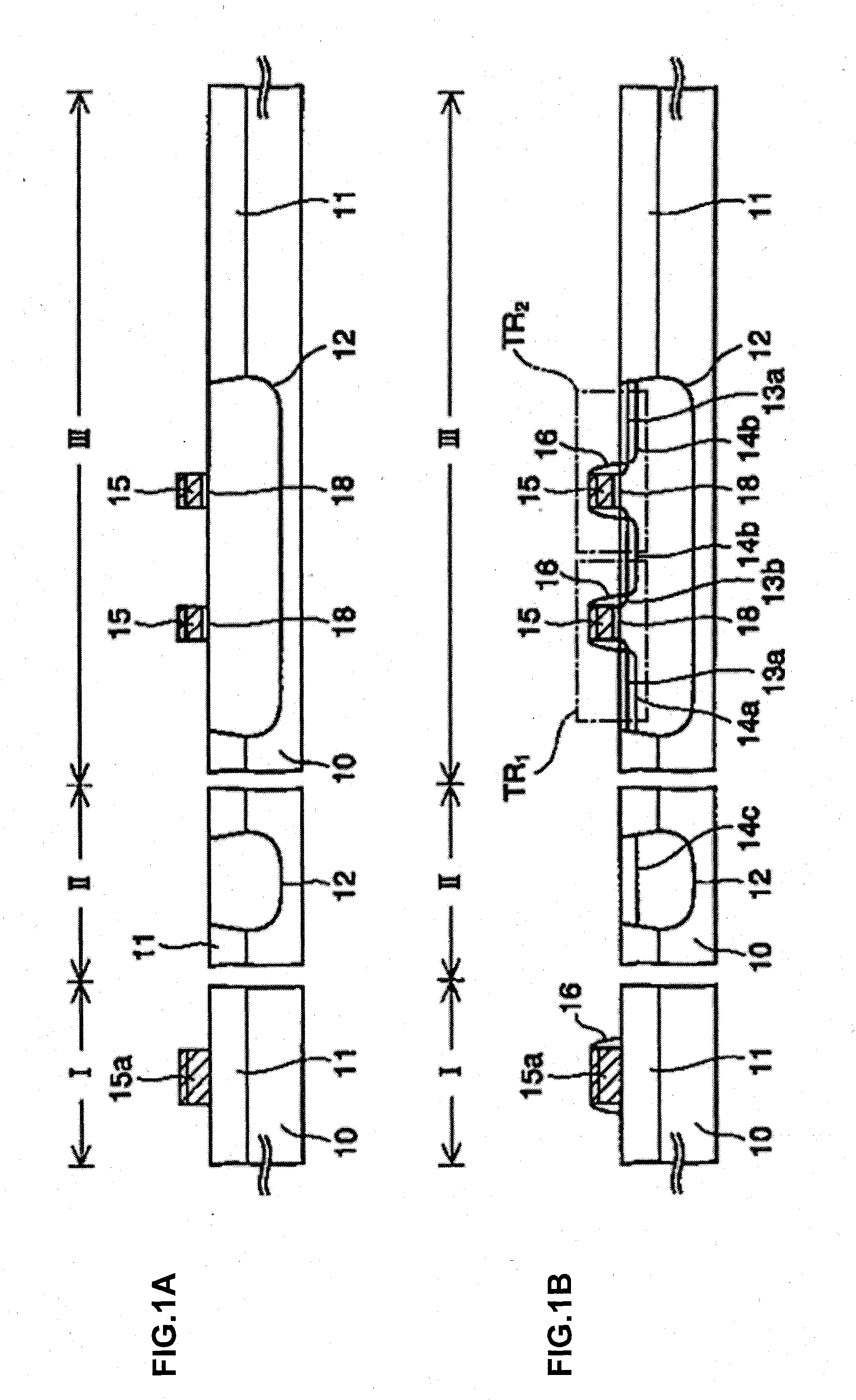
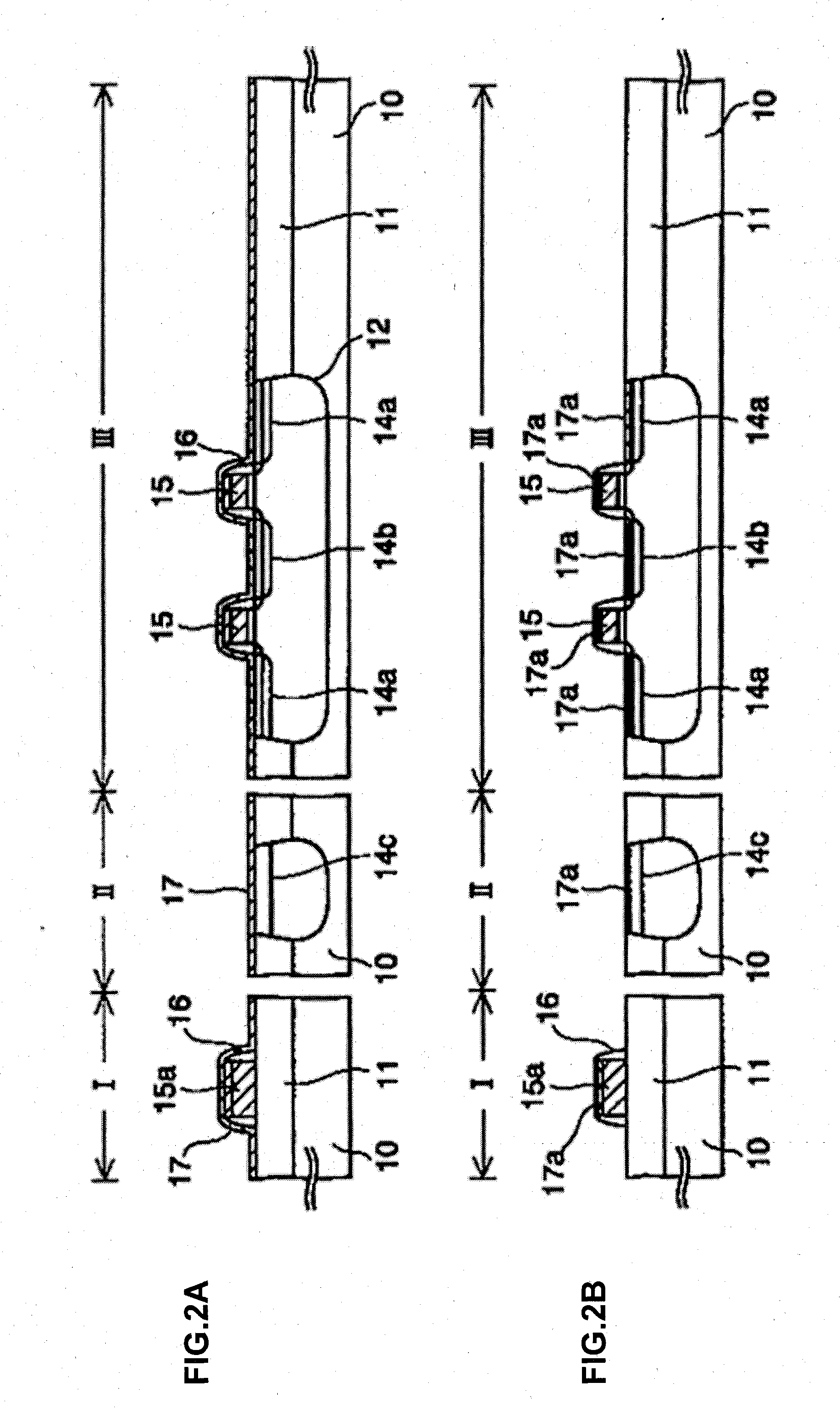
[0032]The cross-sectional structure shown in FIG. 1A is produced by the steps described below.

[0033]First, trenches for shallow trench isolation (STI) are formed on the surface of an n-type or p-type silicon (semiconductor) substrate 10 in order to define an active region of a transistor and the like. An element separation insulating film 11 is formed by embedding an insulating film such as a silicon oxide film in the trenches for STI. The method of forming the element separation ...


PUM


Abstract

A semiconductor device has a conductive film formed over a substrate, an insulating film formed over the conductive film, and having a hole on the conductive film, and a conductive plug formed in the hole including a barrier metal film and a conductive film. A nitride concentration of the barrier metal film is decreased towards an interface between the barrier metal film and the conductive film, and the nitride concentration of the side of the barrier metal film is higher than the nitride concentration of the side of the conductive film at the interface.

Description

BACKGROUND OF THE INVENTION[0001]1. Field of the Invention[0002]The present invention relates to a semiconductor device and a method of producing the same.[0003]2. Description of the Related Art[0004]In semiconductor devices such as LSIs, in order to establish electrical connection between layers, conductive plugs are formed in holes in an interlayer insulating film. For example, in a MOS transistor formed on a semiconductor substrate, conductive plugs are formed on impurity diffusion regions, such as source / drain regions, and gate electrodes. In general, a metal silicide layer is formed on a surface layer of such impurity diffusion regions in order to decrease the contact resistance between the impurity diffusion regions and the conductive plugs.[0005]The above-mentioned conductive plugs are mainly composed of tungsten. However, when tungsten diffuses in an interlayer insulating film disposed on the peripheries of the tungsten plugs, a problem of an increase in the leakage current ...

Claims


Application Information

Patent Timeline
IPC IPC(8): H01L27/00H01L21/00
CPCH01L21/28518H01L21/76816H01L21/76826H01L21/76828H01L21/76832H01L29/7833H01L21/76846H01L21/76856H01L27/11502H01L27/11507H01L28/55H01L21/76834H10B53/30H10B53/00H01L21/28
Inventor NAKAMURA, KOHASEGAWA, TAKASHISUGIYAMA, YOSHIHIROITO, HIDEKI
Owner FUJITSU SEMICON LTD
Why Eureka
Try Eureka