Semiconductor device and method of disconnecting fuse element

a technology of a fuse element and a semiconductor, applied in the field of semiconductor devices, can solve the problems of increasing the actual situation of the number of defective memory cells included in one chip, increasing the chip area, and increasing the risk of breaking at this part, so as to reduce the influence of adjacent fuse elements and their periphery, reduce damage applied to various lower-layer wirings and to the semiconductor substrate, and efficiently attenuate the laser beam

Active Publication Date: 2008-07-31
MICRON TECH INC
View PDF7 Cites 5 Cited by
  • Summary
  • Abstract
  • Description
  • Claims
  • Application Information

AI Technical Summary

Benefits of technology

[0022]According to the present invention, the attenuation members attenuate unnecessary energy of a laser beam. Therefore, at the time of disconnecting a predetermined fuse element, influence given to the adjacent fuse element and its periphery can be decreased. Accordingly, a layout pitch of the fuse elements can be narrowed while securing reliability. Even when only one fuse element is laid out, the energy of the laser beam spread to below the fuse element can be attenuated. Consequently, damage applied to various lower-layer wirings and to the semiconductor substrate can be decreased.
[0023]When columnar bodies extending to a direction approximately perpendicular to the semiconductor substrate are used as the attenuation members, the columnar bodies themselves can absorb the energy of the laser beam

Problems solved by technology

However, along the progress of microfabrication, the number of defective memory cells included in one chip also increases in the actual situation.
This has a disadvantage of increasing a chip area.
For example, when the through-hole electrode 12b pierces through a part of an insulation layer having a high light-absorbing rate like a silicon nitride film, the through-hole electrode 12b has a risk of being broken at this part.
Therefore, when the layout pitch P of the fuse element is narrowed, this has a problem of a reduc

Method used


Image

  • Semiconductor device and method of disconnecting fuse element
  • Semiconductor device and method of disconnecting fuse element
  • Semiconductor device and method of disconnecting fuse element

Examples


Embodiment Construction

[0041]Preferred embodiments of the present invention will now be explained below in detail with reference to the accompanying drawings.

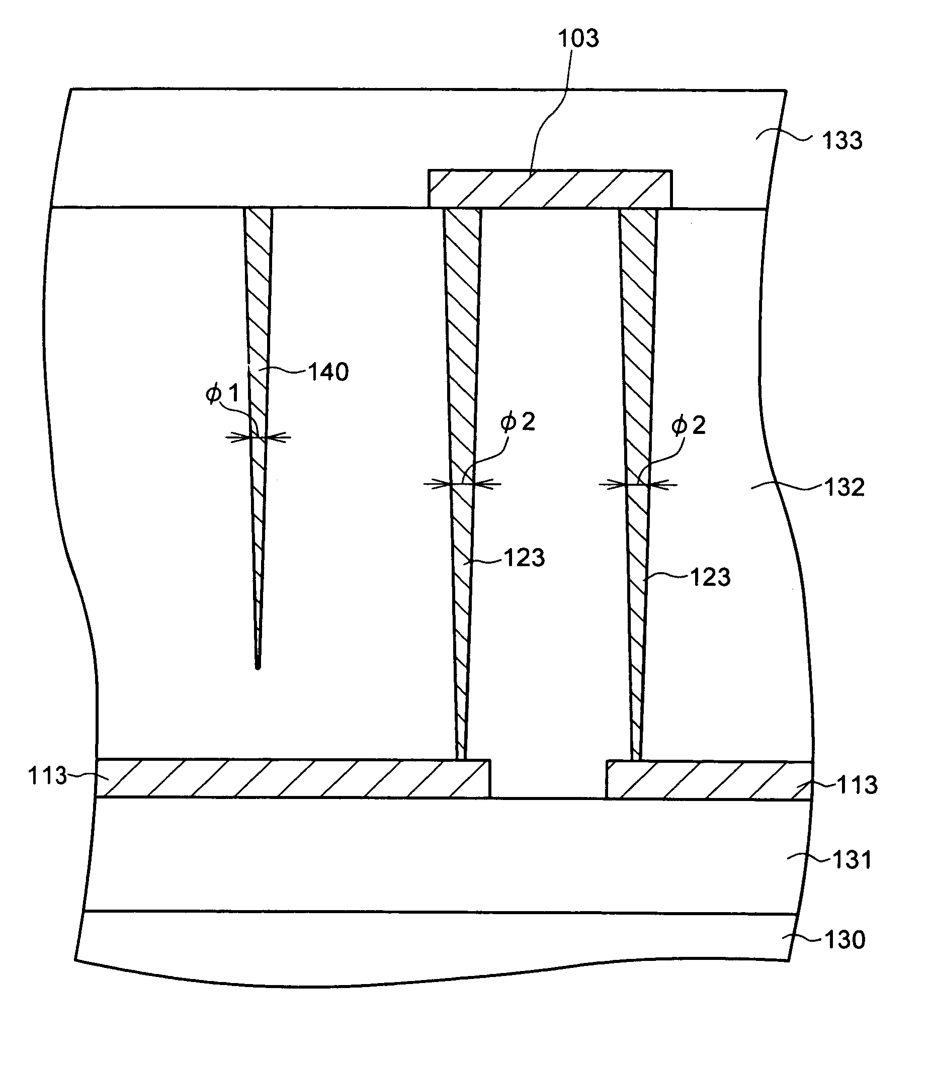
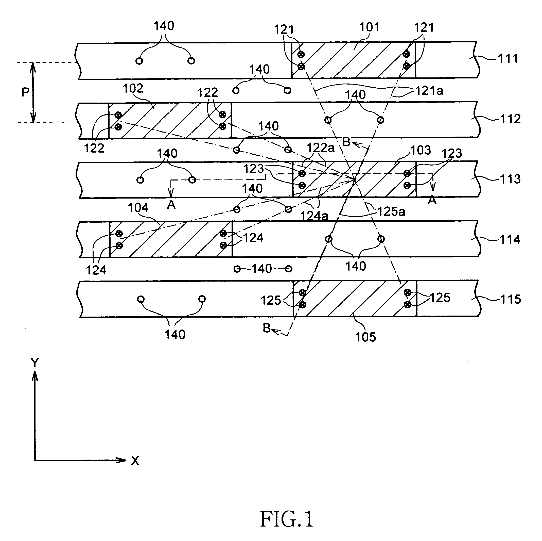
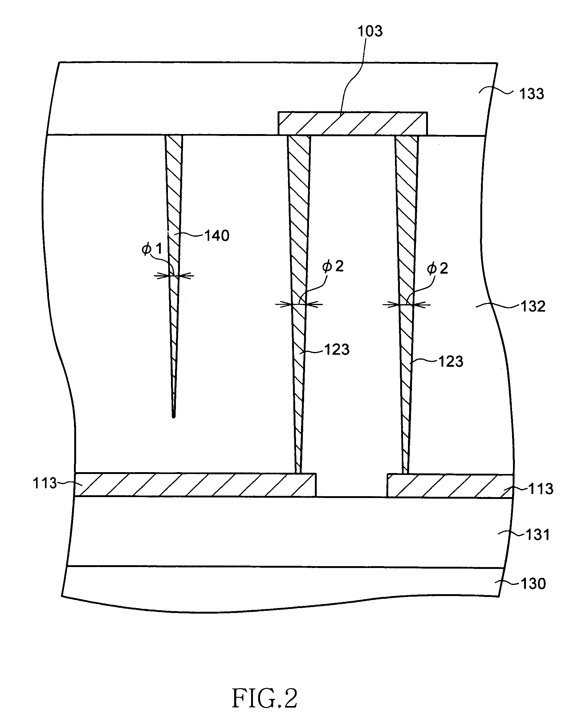
[0042]FIG. 1 is a schematic top plan view showing a configuration of main parts of a semiconductor device according to one embodiment of the present invention. FIG. 2 is a schematic cross-sectional view along a line A-A shown in FIG. 1, and FIG. 3 is a schematic cross-sectional view along a line B-B shown in FIG. 1.

[0043]As shown in FIG. 1, the semiconductor device according to the present embodiment has plural fuse elements 101 to 105. The fuse elements 101 to 105 are connected to lower-layer wirings 111 to 115 extending to the X direction, respectively.

[0044]In the present embodiment, the fuse elements 101 to 105 connected to the adjacent lower-layer wirings 111 to 115 are deviated to the X direction, respectively. That is, the fuse elements 101 to 105 are laid out in zigzag manner. This layout is made to secure high degree of location and to incre...


PUM


Abstract

A semiconductor device includes plural fuse elements which can be disconnected by irradiating a laser beam, and attenuation members which are located between the plural fuse elements as viewed two-dimensionally and can attenuate the laser beam. Each attenuation member includes plural columnar bodies. With this arrangement, the attenuation members including plural columnar units absorb the laser beam leaked out from a fuse element to be disconnected to a semiconductor substrate side. The laser beam is also scattered by Fresnel diffraction. Therefore, the columnar body can efficiently attenuate the laser beam, without generating a crack in the insulation film by absorbing excessive energy.

Description

TECHNICAL FIELD[0001]The present invention relates to a semiconductor device, and more particularly relates to a semiconductor device having a fuse element which can be disconnected by irradiating a laser beam to this fuse element. The present invention also relates to a method of disconnecting a fuse element, and more particularly relates to a method of disconnecting a fuse element by irradiating a laser beam to this fuse element.BACKGROUND OF THE INVENTION[0002]A memory density of semiconductor memory devices as represented by a DRAM (Dynamic Random Access Memory) increases year by year based on progress of microfabrication. However, along the progress of microfabrication, the number of defective memory cells included in one chip also increases in the actual situation. These defective memory cells are usually replaced by redundant memory cells, thereby relieving defective addresses.[0003]In general, defective addresses are stored in a program circuit including plural fuse elements...

Claims


Application Information

Patent Timeline
IPC IPC(8): H01L29/00
CPCG11C17/14H01L23/5258H01L2924/0002H01L2924/00
Inventor OGAWA, SUMIO
Owner MICRON TECH INC
Why Eureka
Try Eureka