Mounting terminal substrate and display device using the same

Active Publication Date: 2008-07-31
TRIVALE TECH
View PDF3 Cites 29 Cited by
  • Summary
  • Abstract
  • Description
  • Claims
  • Application Information

AI Technical Summary

Benefits of technology

[0012]According to the aspect of the present invention, the margin of positional alignment error in COG mounting can be made greater,

Problems solved by technology

A liquid-crystal display device is thin, light weight, and power-thrifty and used as display devices of many pieces of equipment.
TAB mounting encounters difficulty at such a narrow pitch.
Consequently, a margin of error in positional alignment between the bumps provided on the driver IC and the opening section located above the mounting terminal has become smaller, and there has arisen a problem of a failure to fit the bumps into the opening section when positional displacement having occurred during COG mounting is great.
If the bumps fail to fit into the opening section and rest on an insulation film located around the opening section, the following problem will arise.
In mounting of the driver IC by way of the ACF, an overlap area between the bumps and the mounting terminals is reduced, and hence occurrence of a failure of electrical conduction is increased as a result of a decrease in the number of conductive partic

Method used


Image

  • Mounting terminal substrate and display device using the same
  • Mounting terminal substrate and display device using the same
  • Mounting terminal substrate and display device using the same

Examples


first embodiment

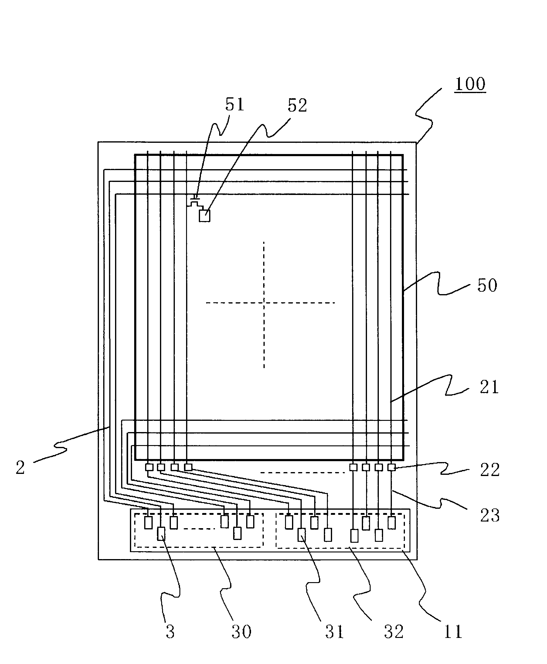
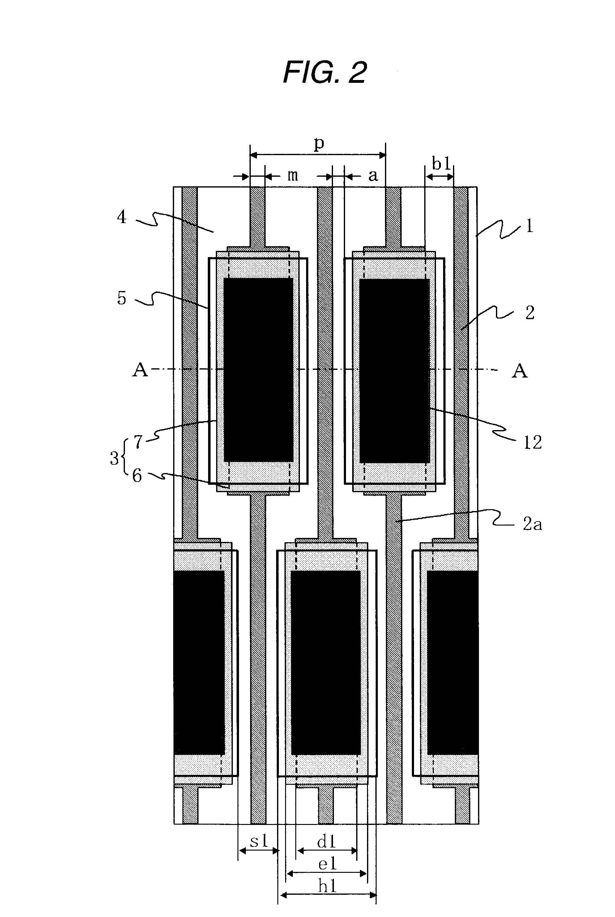
[0022]FIG. 1 is a plan view showing the general configuration of a mounting terminal substrate of a liquid-crystal display device of a first embodiment. FIG. 2 is a plan view showing a gate mounting terminal area of the mounting terminal substrate of the first embodiment. FIG. 3 is a cross-sectional view taken along cutting plane A-A shown in FIG. 2.

[0023]In FIG. 1, a pixel area 50 is provided in amounting terminal substrate 100 which constitutes a portion of the liquid-crystal display device and opposes a color filter substrate by way of a liquid-crystal layer. A plurality of gate lines 2 and source lines 21, which intersect at right angles, are provided in the pixel area 50, and a switching element 51 formed from a thin-film transistor, or the like, and a pixel electrode 52, or the like, are formed in a pixel (only one pixel is illustrated) located at each of the intersections. The plurality of gate lines 2 and the source lines 21 are drawn from the pixel area 50. A gate mounting ...

second embodiment

[0056]A second embodiment relates to a configuration of the top layer of the insulation film 4 being the organic resin film 4c and the upper conductive film 7 being ITO. ITO formed on an organic substance differs from ITO formed on an inorganic substance in terms of film quality and an etch rate. An etch rate of the ITO formed on an organic substance is two to eight times as high as an etch rate of the ITO formed on an inorganic substance.

[0057]Since the two types of ITO greatly differ from each other in terms of an etch rate, etching of ITO must be divided into two operations in the first embodiment in order to process, with superior dimensional accuracy, the pixel electrodes 52 made from ITO formed on the organic resin film 4c and the upper conductive film 7 made from ITO. After etching of the pixel electrodes 52 whose etch rate is high, the ITO still remaining on the glass substrate 1 within the opening sections 5 is removed by means of additional etching while the pixel electrod...

third embodiment

[0061]FIG. 7 is a cross-sectional view showing a gate mounting terminal area of a third embodiment. An inorganic insulation film 4d formed from an oxide film or a nitride film is formed additionally on the organic resin film 4c forming the insulation film 4. The top layer of the insulation film 4 is formed as the inorganic insulation film 4d, thereby rendering the etch rate of the pixel electrodes 52 and the etch rate of the upper conductive films 7, which are formed from different types of ITO, uniform and enhancing dimensional accuracy. Since ITO is formed on the inorganic substance by means of such a configuration, the etch rate becomes low. However, an advantage of the ability to form the pixel electrodes 52 and the upper conductive films 7 in their originally-designed positions by means of single etching of ITO without involvement of the remaining ITO films 7a is yielded with superior accuracy.

[0062]Incidentally, the organic resin film 4c adjoins respective side surfaces of the...


PUM


Abstract

A mounting terminal substrate includes a substrate, mounting terminals arranged in staggered rows on the substrate, each mounting terminals includes a lower conductive film and an upper conductive film, lines that are provided between the mounting terminals in a direction of a row, an insulation film that covers the lines, and opening sections on the respective mounting terminals from which the insulation films are removed, wherein a width of the upper conductive film in the direction of the row is greater than a width of the lower conductive film in the direction of the row so as to cover the lower conductive films exposed through the opening sections and is equal to or smaller than a width of the opening section in the direction of the row.

Description

[0001]This application claims priority from Japanese Patent Application No. 2006-198939 filed on Jul. 21, 2006, the entire subject matter of which is incorporated herein by reference.BACKGROUND OF THE INVENTION[0002]1. Field of the Invention[0003]The present invention relates to a mounting terminal substrate having a mounting terminal provided on a substrate and a display device using the substrate, for example, a mounting terminal substrate which can be appropriately utilized for a liquid-crystal display device.[0004]2. Description of the Related Art[0005]A liquid-crystal display device is thin, light weight, and power-thrifty and used as display devices of many pieces of equipment. A chip-on glass (COG) mounting technique for mounting a driver IC for the purpose of driving liquid-crystal directly on a glass substrate on which are formed mounting terminals is frequently used for middle-size and small-size liquid-crystal display devices. In COG mounting, electrical conduction is oft...

Claims


Application Information

Patent Timeline
IPC IPC(8): G02F1/1343
CPCG02F1/13452G02F1/13458H01L2224/73204G02F2001/13456G02F1/136286G02F1/13456G02F1/1345
Inventor YASUDA, SHOHEIHASHIGUCHI, TAKAFUMIUEDA, SEIYA
Owner TRIVALE TECH
Why Eureka
Try Eureka