Anisotropic conductive film, joined structure, and connecting method

Inactive Publication Date: 2012-10-18
DEXERIALS CORP
View PDF5 Cites 9 Cited by
  • Summary
  • Abstract
  • Description
  • Claims
  • Application Information

AI Technical Summary

Benefits of technology

[0022]The present invention aims to solve the various problems in the art, and to achieve the following object. An object of the present invention is to provide an anisotropic conductive film having both high bonding strength under the conditions of low temperature and short period, and excellent conduction reliability, and to provide a joined structure and connecting method using the anisotropic conductive film.
[0046]The present invention can solve the various problems in the art, achieve the aforementioned object, and can provide an anisotropic conductive film having both high bonding strength under the conditions of low temperature and short period, and excellent conduction reliability, as well as providing a joined structure and connecting method using the anisotropic conductive film.

Problems solved by technology

As the pitch becomes finer, however, it is more difficult to accurately position and align the patterns during thermal pressure bonding with the ACF.
On the other hand, the latter is difficult to position because the glass of the PWB and the thickness of the epoxy material are not qualitatively stable and the thermal expansion degree thereof is not stable.
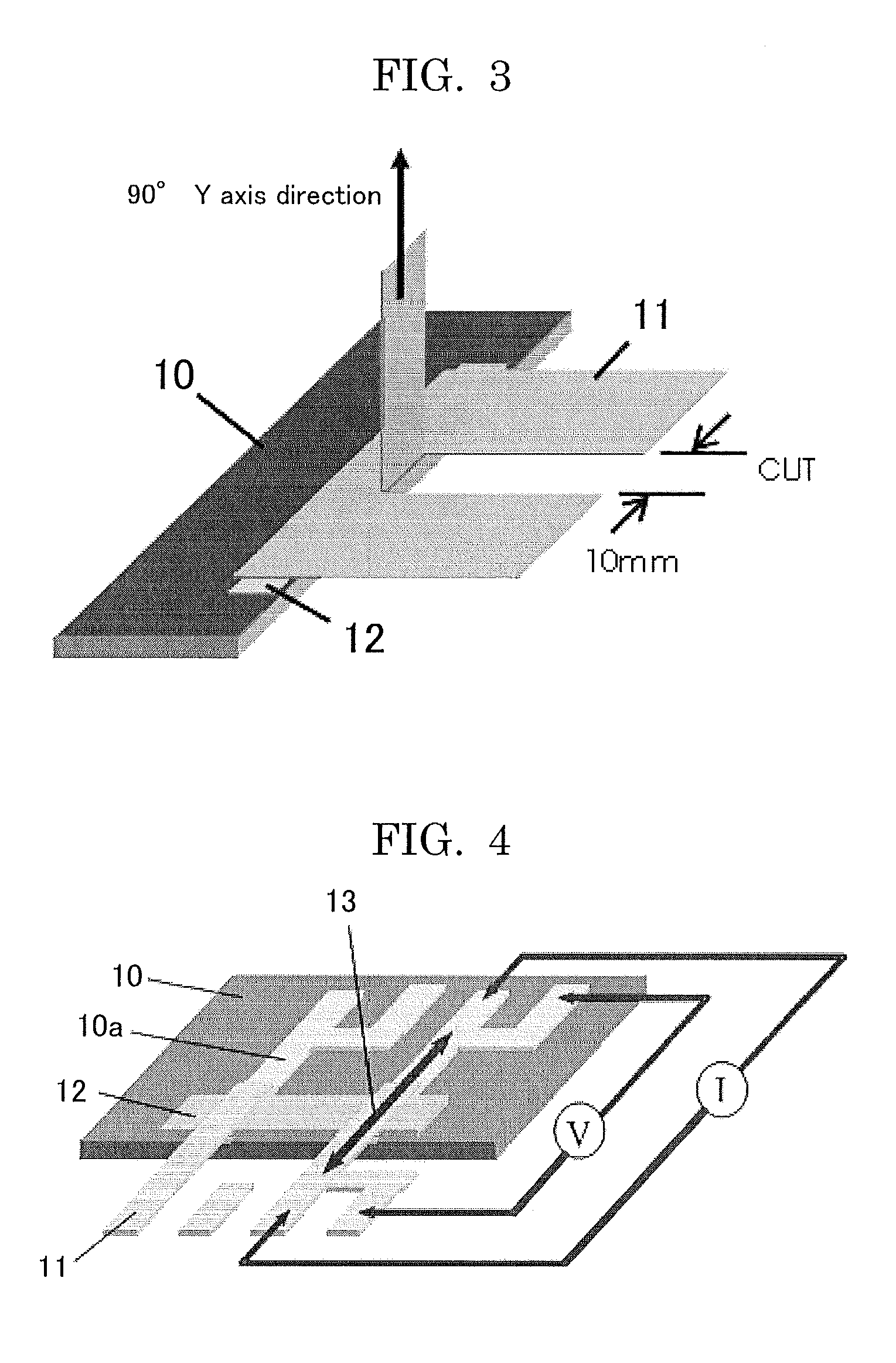
If low temperature bonding and short period bonding abilities are imparted to the ACF and the mechanical strength of the binder cured product of the ACF is enhanced to improve the conduction reliability, however, the bonding strength (peel strength in the 90° Y axis direction) at the bonding part between the COF and PWB tends to be low.
This is probably because the polyimide material of the COF and the binder o the ACF do not sufficiently wet and it is difficult to form chemical bonding between these materials as the binder is quickly cured in the low temperature region, and because the deformability of the binder cured product itself is low in the bonding part when the peel strength in the 90° Y axis direction and the absorption energy for deforming is low, as the binder cured product is hard.
If the mechanical strength (i.e. elastic modulus) of the binder cured product is designed low to enhance the deformability of the binder cured product in the bonding part during the measurement of the peel strength in the 90° Y axis direction, the bonding strength increases, but the conduction reliability is impaired.
As mentioned above, to balance out between the improvement of the bonding strength with the COF and the improvement of the conduction reliability of a tape carrier package (TCP) is one of the extremely difficult problems to be solved.
Moreover, there is a problem that a sufficient peel strength cannot be attained depending on a type of the COF.
If the formula is optimized for one particular COF, however, such an ACF may be difficult to adhere to other COFs.
In this case, however, the binder tends to be loosen in the high temperature high humidity environment (85° C., 85% RH), and therefore there is a problem of increasing the conduction resistance.
In any of the prior art documents, however, an anisotropic conductive film having high bonding strength under the conditions of low temperature and short time (at 130° C. for 3 seconds) and excellent conduction reliability, as well as a joined structure and connection method using such the anisotropic conductive film have not been provided yet.

Method used


Image

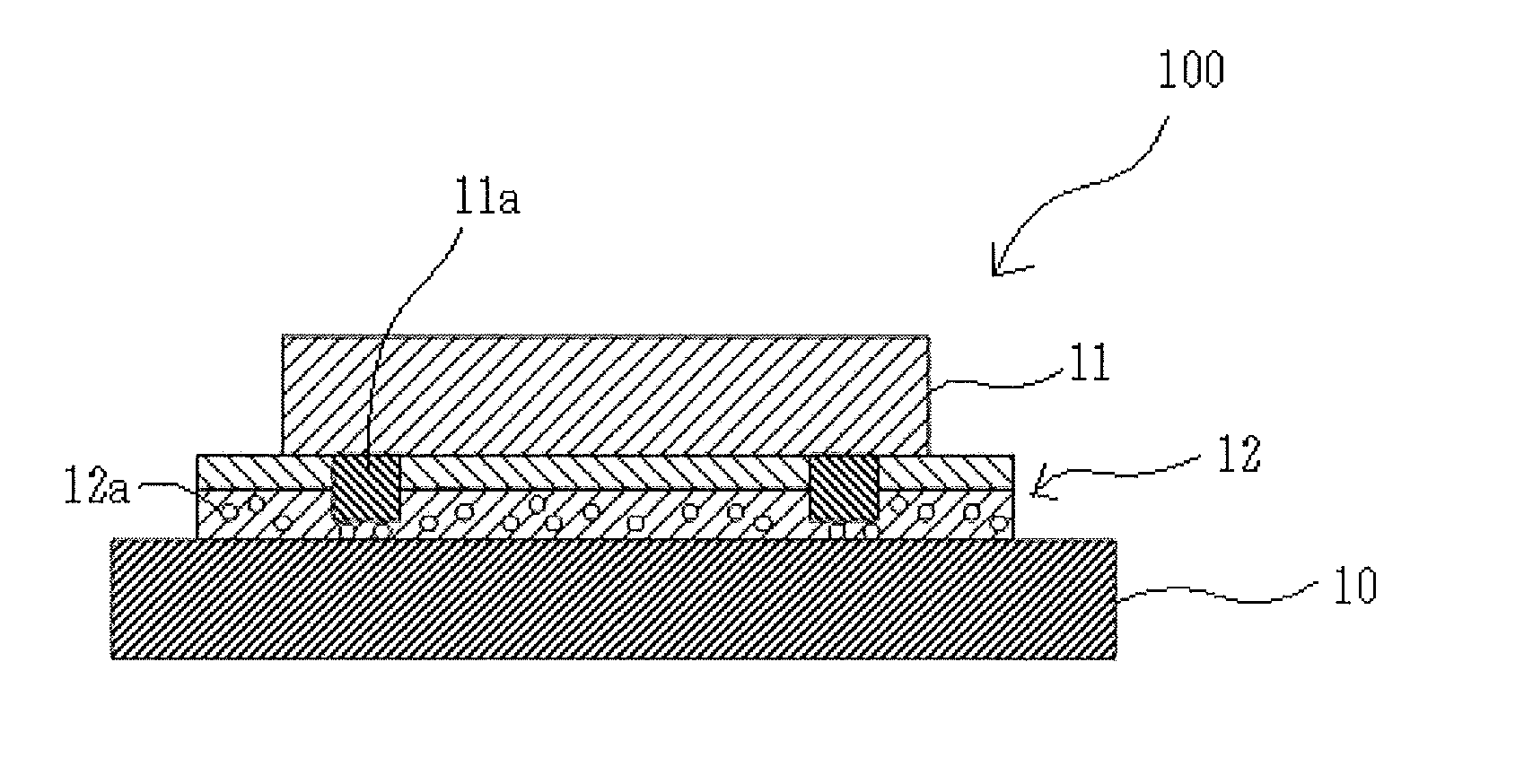
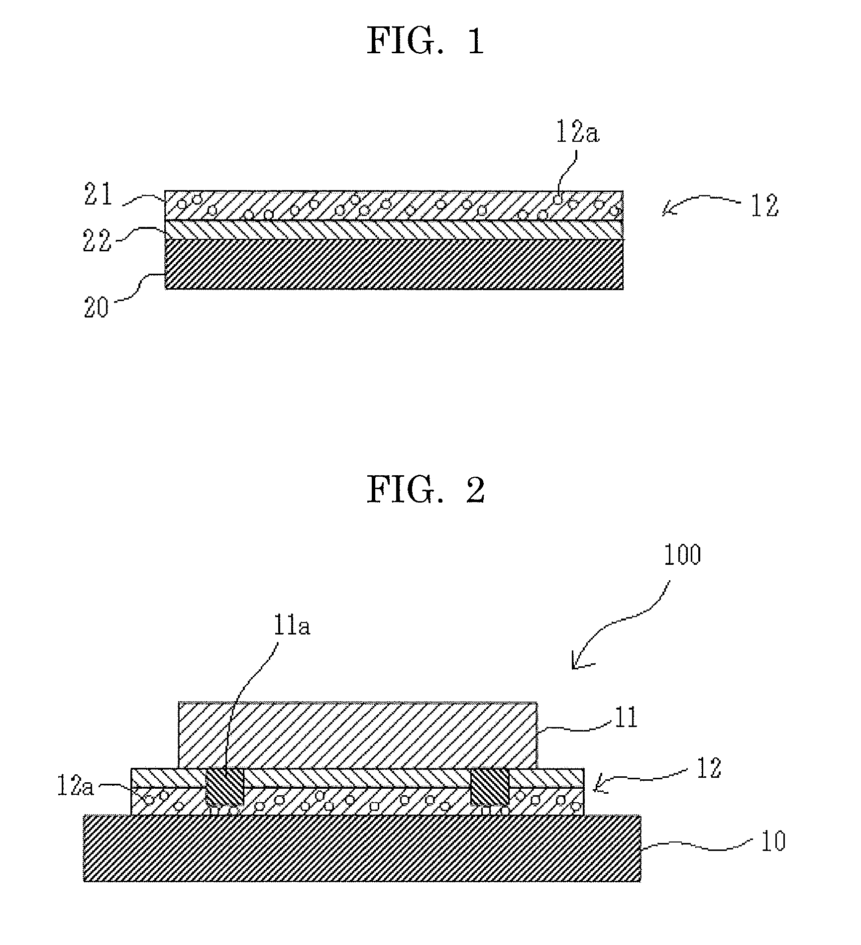
  • Anisotropic conductive film, joined structure, and connecting method
  • Anisotropic conductive film, joined structure, and connecting method
  • Anisotropic conductive film, joined structure, and connecting method

Examples


production example 1

—Production of Ni Particles—

[0111]Nickel Powder Type T255 of Vale Inco was classified to give the average particle diameter of 3 μm, to thereby obtain Ni particles.

production example 2

—Production of Au-Plated Ni Particles—

[0112]After classifying Nickel Powder Type T255 of Vale Inco to give the average particle diameter of 3 μm, the resulting Ni particles were subjected to displacement plating to plate Au on surfaces of the Ni particles, to thereby produce Au-plated Ni particles.

production example 3

—Production of Ni-Plated Resin Particles—

[0113]Resin particles of a styrene-divinyl benzene copolymer having the average particle diameter of 10 μm were subjected to electroless plating to plate Ni on surfaces of the resin particles, to thereby produce Ni-plated resin particles.

Production Example 4

[0114]—Production of Ni / Au-Plated Resin Particles A—

[0115]Resin particles of a styrene-divinylbenzene copolymer having the average particle diameter of 10 μm were subjected to electroless plating to plate Ni on surfaces of the resin particles. The resulting particles were further subjected to displacement plating to plate Au on the Ni-plated surface, to thereby produce Ni / Au-Plated Resin Particles A.


PUM

PropertyMeasurementUnit
Fractionaaaaaaaaaa
Percent by massaaaaaaaaaa

Abstract

To provide an anisotropic conductive film, which contains: an electric conductive layer containing Ni particles, metal-coated resin particles, a binder, a polymerizable monomer, and a curing agent; and an insulating layer containing a binder, a monofunctional polymerizable monomer, and a curing agent, wherein the metal-coated resin particles are resin particles each containing a resin core coated at least with Ni.

Description

CROSS-REFERENCE TO RELATED APPLICATION[0001]This is a continuation of Application No. PCT / JP2011 / 051008, filed on Jan. 20, 2011.BACKGROUND OF THE INVENTION[0002]1. Field of the Invention[0003]The present invention relates to an anisotropic conductive film having both high conduction reliability and high bonding strength, which is particularly suitable for connecting COF with PWB, and relates to a joined structure and connecting method using the anisotropic conductive film.[0004]2. Description of the Related Art[0005]When a driver IC is fabricated on a liquid crystal display (LCD), as a common method, a COF (Chip On Film), on which the driver IC has been fabricated on a flexible board (FPC) in advance, is thermally bonded to the LCD and to a printed wiring board (PWB) via an anisotropic conductive film (ACF).[0006]In this case, electric connection between the LCD and the COF, or the COF and the PWB can be achieved by bonding them with the ACF. In addition, insulating properties can b...

Claims


Application Information

Patent Timeline
IPC IPC(8): H05K1/18H05K1/03C09J7/10
CPCC08G2650/56C08K9/02H01L2924/01029H01L2924/00013H01L2224/32225H01L2224/29444H01L2224/83862H01L2224/83851H01L2224/83201H01L2224/81191H01L2224/29499H01L2224/29355H01L2224/2929H01L2224/2919H01L2224/29082H01L24/83H01L24/29H01L2224/29455H01L2224/2939C09J2461/00C09J2433/00C09J2205/102C09J2203/326C09J2201/36C09J11/02C09J9/02C09J7/00C09J5/06C08L71/00C08K2003/0862C08K3/08C08L33/06H01L2924/00014H01L2224/13099H01L2224/13599H01L2224/05599H01L2224/05099H01L2224/29099H01L2224/29599H01L2924/0665H01L2924/15788H01L2924/14C09J7/10C08K2201/001C09J2301/208C09J2301/408H01L2924/00G02F1/1345H01B5/16C09J4/00C09J11/06
Inventor YAMADA, YASUNOBUMIYAUCHI, KOICHI
Owner DEXERIALS CORP
Why Eureka
Try Eureka