This helps you quickly interpret patents by identifying the three key elements:
Problems solved by technology
Method used
Benefits of technology
Benefits of technology
The present invention provides a multilayer wiring substrate that can achieve excellent conduction reliability. This is achieved by preventing deformation of conductive paths and ensuring that adjacent conductive paths do not come into contact with each other. The invention provides a reliable and reliable substrate for use in various electronic devices.
Problems solved by technology
Particularly, downsizing of electronic components such as a semiconductor element remarkably occurs, and since conventional methods such as wire bonding in which wiring substrates are directly connected cannot secure sufficient connection stability, an anisotropic conductive member is attracting attention as an electronic connection member.
Method used
Image
Click on the blue label to locate the original text in one second.
Reading with bidirectional positioning of images and text.
Examples
examples
[0222]Hereinafter, the present invention will be described specifically with reference to the following examples. However, the present invention is not limited thereto.
[0223]First, the preparation of the anisotropic conductive member and the wiring substrate used in each example will be described.
[0224][Preparation of Anisotropic Conductive Member]
[0226]Molten metal was prepared using an aluminum alloy containing Si: 0.06% by mass, Fe: 0.30% by mass, Cu: 0.005% by mass, Mn: 0.001% by mass, Mg: 0.001% by mass, Zn: 0.001% by mass, and Ti: 0.03% by mass, and a balance consisting of Al and unavoidable impurities and a molten metal treatment and filtration were carried out. Then, an ingot having a thickness of 500 mm and a width of 1,200 mm was prepared by a direct chilling casting (DC) method.
[0227]Next, the surface of the resulted ingot was cut by a facing machine so as to have an average thickness of 10 mm and then heated at 550° C. for about...
examples 1 to 7
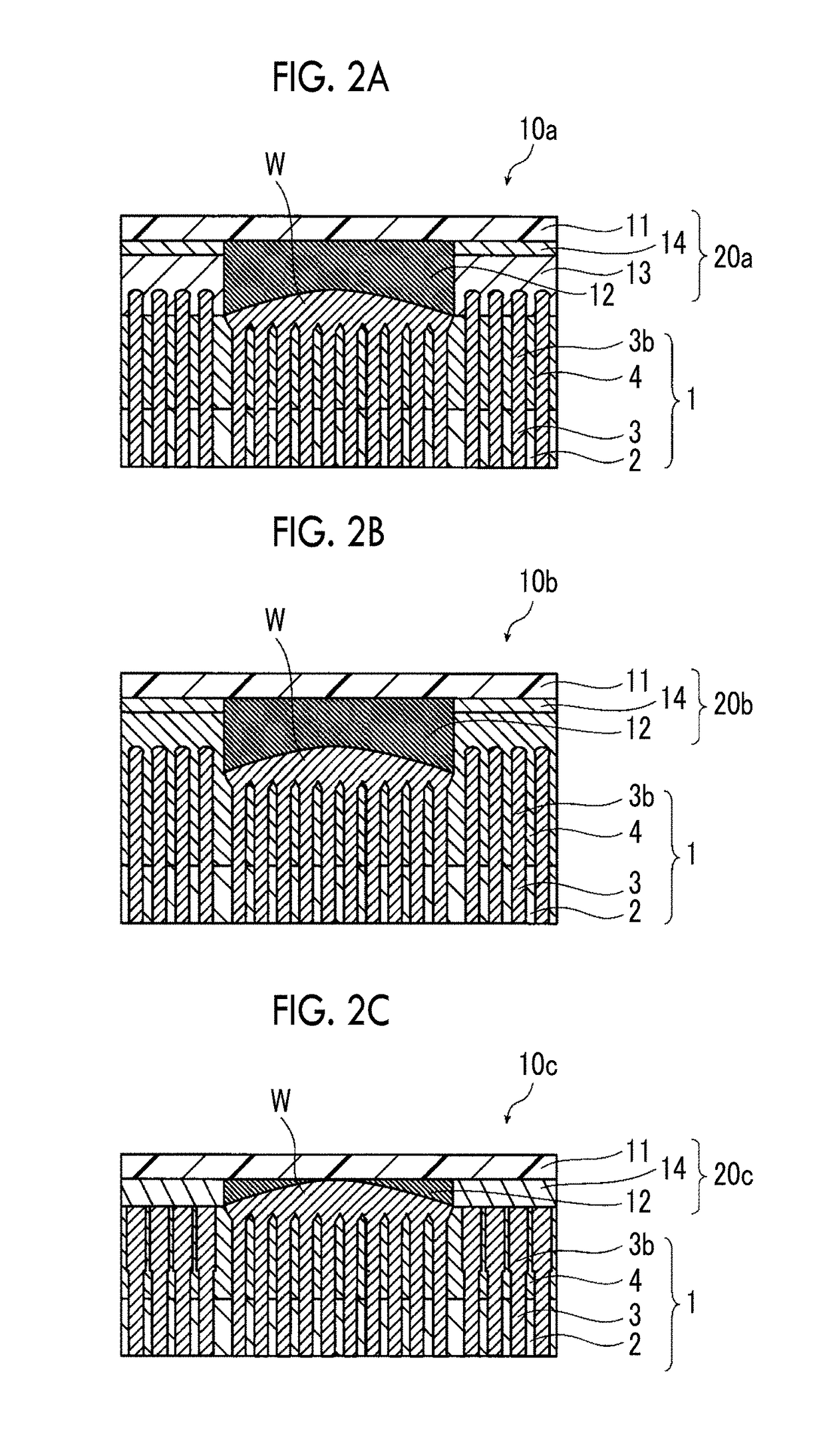
[0291]For Examples 1 to 7, multilayer wiring substrates having the configuration shown in FIG. 2B were repapered.
[0292]The TEG chip (B) having a step between the passivation layer and the Cu pad surface was used as a wiring substrate. The step between the passivation layer and the Cu pad surface was 50 nm.
[0293]The TEG chop (B) and the anisotropic conductive member were laminated in this order and bonded using a room temperature bonding apparatus (WP-100, manufactured by PMT Corporation) under the conditions shown in Table 1 and the condition of retaining for 5 minutes to prepare a sample of a multilayer wiring substrate.
[0294]When the bonding portion of each prepared multilayer wiring substrate was cut with FIB in a thickness direction and the cross section thereof was observed by capturing a surface image (magnification: 50,000 times) of the cross-section with FE-SEM, adjacent conductive paths of the conductive paths coming into contact with the electrode came into contact with ea...
example 8
[0295]For Example 8, a multilayer wiring substrate having a configuration shown in FIG. 2B was prepared.
[0296]That is, the multilayer wiring substrate was prepared in the same manner as in Example 5 except that the step between the passivation layer and the Cu pad surface of the TEG chip (B) was set to 150 nm.
[0297]When the bonding portion of the prepared multilayer wiring substrate was cut with FIB in a thickness direction and the cross section thereof was observed by capturing a surface image (magnification: 50,000 times) of the cross-section with FE-SEM, adjacent conductive paths of the conductive paths coming into contact with the electrode came into contact with each other and the conductive paths not coming into contact with the electrode were embedded in the pressure sensitiveadhesive layer not to come into contact with other conductive paths.
PUM
Abstract
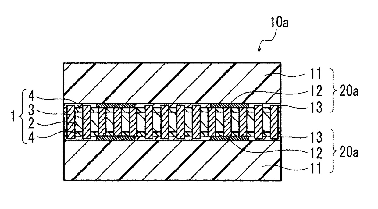
Provided is a multilayer wiring substrate capable of achieving excellent conduction reliability. The multilayer wiring substrate is formed by laminating an anisotropic conductive member including an insulating base which is made of an inorganic material, a plurality of conductive paths which are made of a conductive member, penetrate the insulating base in a thickness direction thereof and are provided in a mutually insulated state, and a pressure sensitiveadhesive layer which is provided on a surface of the insulating base, in which each conductive path has a protrusion protruding from the surface of the insulating base, and a wiring substrate having a substrate and one or more electrodes to be formed on the substrate, and conductive paths which come into contact with the electrode among the plurality of conductive paths are deformed so that adjacent conductive paths come into contact with each other.
Description
CROSS-REFERENCE TO RELATED APPLICATIONS[0001]This application is a Continuation of PCT International Application No. PCT / JP2015 / 085399 filed on Dec. 17, 2015, which claims priority under 35 U.S.C. §119(a) to Japanese Patent Application No. 2014-257473 filed on Dec. 19, 2014. The above application is hereby expressly incorporated by reference, in its entirety, into the present application.BACKGROUND OF THE INVENTION1. Field of the Invention[0002]The present invention relates to a multilayer wiring substrate.2. Description of the Related Art[0003]A metal-filled microstructure (device) that is obtained by filling micropores provided in an insulating base with a metal is one of the fields which have attracted attention in recent nanotechnologies. For example, it is expected that a metal-filled microstructure will be used for an anisotropic conductive member.[0004]This anisotropic conductive member is inserted between an electronic component such as a semiconductor element and a circuit ...
Claims
Application Information
Patent Timeline
Application Date:The date an application was filed.
Publication Date:The date a patent or application was officially published.
First Publication Date:The earliest publication date of a patent with the same application number.
Issue Date:Publication date of the patent grant document.
PCT Entry Date:The Entry date of PCT National Phase.
Estimated Expiry Date:The statutory expiry date of a patent right according to the Patent Law, and it is the longest term of protection that the patent right can achieve without the termination of the patent right due to other reasons(Term extension factor has been taken into account ).
Invalid Date:Actual expiry date is based on effective date or publication date of legal transaction data of invalid patent.

