Anisotropic conductive bonding member, semiconductor device, semiconductor package and semiconductor device production method

a technology of anisotropic conductive and bonding member, which is applied in the manufacture of printed circuit components, printed circuit components, basic electric elements, etc., can solve the problems of thermo compression (thermo compression), semiconductor element remarkably occurring, and downsizing electronic components, and achieve excellent conduction reliability

Active Publication Date: 2018-12-06
FUJIFILM CORP
View PDF4 Cites 2 Cited by
  • Summary
  • Abstract
  • Description
  • Claims
  • Application Information

AI Technical Summary

Benefits of technology

[0045]As described below, according to the present invention, it is possible to provide an anisotropic conductive bonding member capable of achieving excellent conduction reliability and insulation reliability, a semiconductor device using the same, a semiconductor package, and a semiconductor device production method.

Problems solved by technology

Particularly, downsizing of electronic components such as a semiconductor element remarkably occurs and conventional methods such as wire bonding in which wiring substrates are directly connected to each other, flip chip bonding, thermo compression (thermocompression) bonding, and the like cannot secure sufficient connection stability.

Method used


Image

  • Anisotropic conductive bonding member, semiconductor device, semiconductor package and semiconductor device production method
  • Anisotropic conductive bonding member, semiconductor device, semiconductor package and semiconductor device production method
  • Anisotropic conductive bonding member, semiconductor device, semiconductor package and semiconductor device production method

Examples


examples

[0313]Hereinafter, the present invention will be described specifically with reference to the examples. However, the present invention is not limited thereto.

examples 1-1 and 1-2

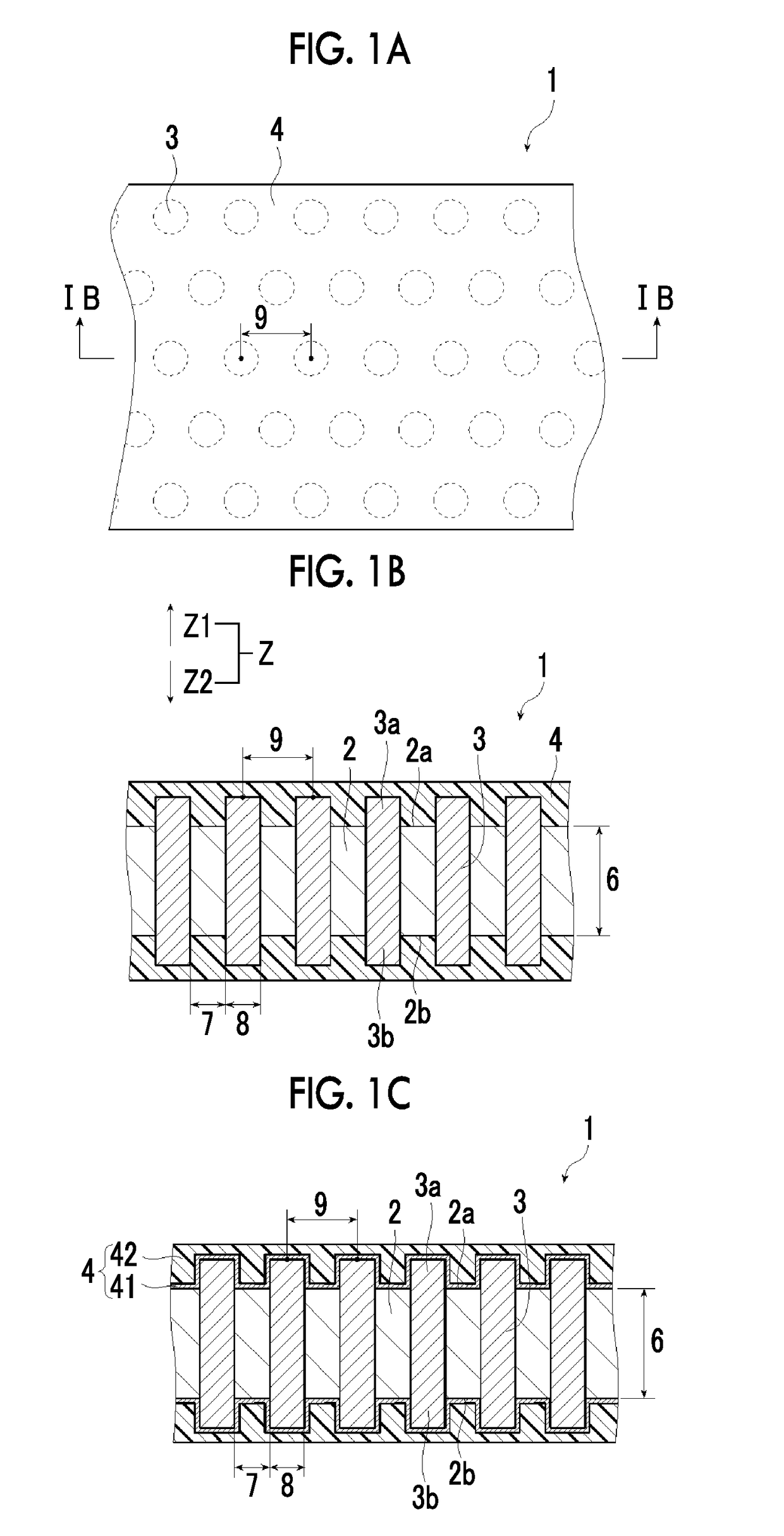
[0314]A commercially available photosensitive glass substrate (trade name: PEG3 manufactured by HOYA Corporation: having a size of 5-inch square and a plate thickness of 0.65 mm) was irradiated with ultraviolet rays with a photo mask closely attached thereto. The conditions for irradiation were such that the wavelength was 320 nm and the exposure amount was 550 mJ / cm2. In addition, for the mask pattern, a mask pattern in which total 90,000 circle patterns each having a diameter of 1 μm were arranged at a pitch of 300 μm in the horizontal and vertical directions was used.

[0315]After the laminate was irradiated with ultraviolet rays, a heat treatment was performed in a heating furnace at 550° C. for 1 hour.

[0316]Then, the surface and the rear surface of the photosensitive glass substrate were ground by a double-side surface grinding machine using abrasive particles made of Al2O3 and having a particle size of #1,000, and further subjected to finishing polishing by a double-side polishi...

example 2 , examples 3-1 to 3-12

Example 2, Examples 3-1 to 3-12, and Examples 4-1 and 4-2

[0348](1) Preparation of Aluminum Substrate

[0349]Molten metal was prepared using an aluminum alloy containing Si: 0.06% by mass, Fe: 0.30% by mass, Cu: 0.005% by mass, Mn: 0.001% by mass, Mg: 0.001% by mass, Zn: 0.001% by mass, and Ti: 0.03% by mass, and a balance consisting of Al and unavoidable impurities and a molten metal treatment and filtration were carried out. Then, an ingot having a thickness of 500 mm and a width of 1,200 mm was prepared by a DC method.

[0350]Next, the surface of the resulted ingot was cut by a facing machine so as to have an average thickness of 10 mm and then heated at 550° C. for about 5 hours to carry out a soaking treatment. When the temperature decreased to 400° C., the ingot was formed into a rolled plate having a thickness of 2.7 mm by using a hot rolling mill.

[0351]Further, the heat treatment was conducted at 500° C. using a continuous annealing machine and then the annealed plate were cold-r...


PUM

PropertyMeasurementUnit
aspect ratioaaaaaaaaaa
heightaaaaaaaaaa

Abstract

An object of the present invention is to provide an anisotropic conductive bonding member capable of achieving excellent conduction reliability and insulation reliability, a semiconductor device using the same, a semiconductor package, and a semiconductor device production method. An anisotropic conductive bonding member of the present invention includes an insulating base which is made of an inorganic material, a plurality of conductive paths which are made of a conductive member, penetrate the insulating base in a thickness direction thereof, and are provided in a mutually insulated state, and a pressure sensitive adhesive layer which is provided on a surface of the insulating base, in which each of the conductive paths has a protrusion protruding from the surface of the insulating base, the protrusion of each of the conductive paths is buried in the pressure sensitive adhesive layer, and the pressure sensitive adhesive layer contains a polymer material and an antioxidant material.

Description

CROSS-REFERENCE TO RELATED APPLICATIONS[0001]This application is a Continuation of PCT International Application No. PCT / JP2017 / 003589 filed on Feb. 1, 2017, which claims priority under 35 U.S.C. § 119(a) to Japanese Patent Application No. 2016-037514 filed on Feb. 29, 2016, Japanese Patent Application No. 2016-168958 filed on Aug. 31, 2016 and Japanese Patent Application No. 2016-183963 filed on Sep. 21, 2016. Each of the above applications is hereby expressly incorporated by reference, in its entirety, into the present application.BACKGROUND OF THE INVENTION1. Field of the Invention[0002]The present invention relates to an anisotropic conductive bonding member, a semiconductor device, a semiconductor package, and a semiconductor device production method.2. Description of the Related Art[0003]A metal-filled microstructure (device) that is obtained by filling micropores provided in an insulating base with a metal is one of the fields which have attracted attention in recent nanotech...

Claims


Application Information

Patent Timeline
Patent Type & Authority Applications(United States)
IPC IPC(8): H01L23/00H01L21/768
CPCH01L24/83H01L24/27H01L24/33H01L21/76877H01L21/76841H05K3/323H05K2201/0154H05K2201/0209H05K2201/10378H05K2203/0278H01L2224/29318H01L2224/29366H01L2224/29384H01L2224/29381H01L2224/29324H01L2224/2937H01L24/32H01L2224/16227H01L2224/29313H01L2224/29499H01L2224/73204H01L2224/81193H01L2224/83191H01L2224/83192H01L2224/9211H01L2224/27003H01L2224/29379H01L2224/81H01L2224/83H01L23/142H01L23/481H01L23/4828
Inventor YAMASHITA, KOSUKE
Owner FUJIFILM CORP
Why Eureka
Try Eureka