Dual gate ldmos device and method

a technology of metal oxides and semiconductor devices, applied in the direction of semiconductor devices, basic electric elements, electrical equipment, etc., can solve the problems of serious challenges, misalignment errors, and current day ldmos devices being further shrunk below about 0.5 m process technology,

Inactive Publication Date: 2008-07-31
NORTH STAR INNOVATIONS
View PDF8 Cites 88 Cited by
  • Summary
  • Abstract
  • Description
  • Claims
  • Application Information

AI Technical Summary

Problems solved by technology

However, major design and process problems prevent current day LDMOS devices from being further shrunk below about 0.5 μm process technology.
Breaking through th

Method used


Image

  • Dual gate ldmos device and method
  • Dual gate ldmos device and method
  • Dual gate ldmos device and method

Examples


first embodiment

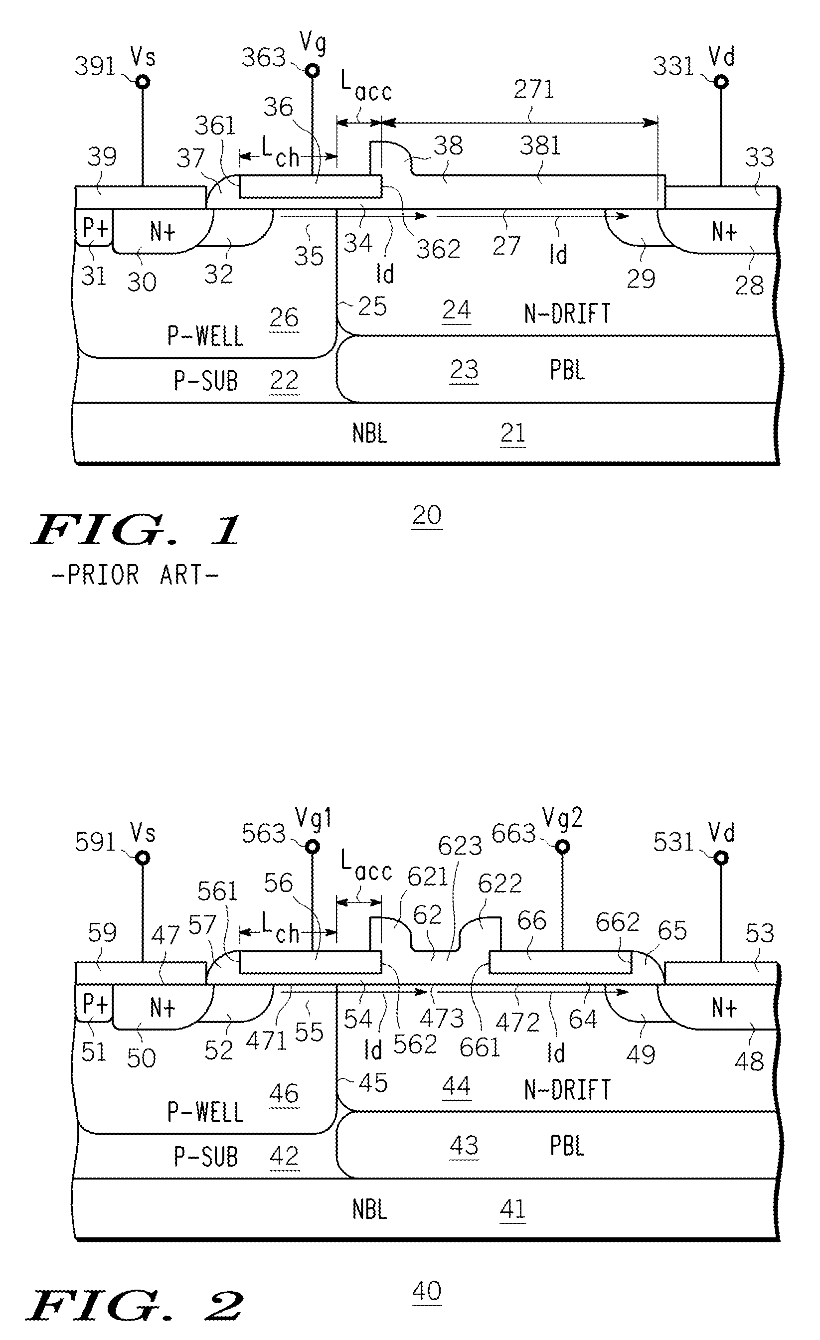
[0044] there is provided a method of fabricating a semiconductor device, comprising the steps of, providing a semiconductor having a substrate region of a first conductivity type and first impurity concentration, extending to a surface of the semiconductor, impurity doping a first region of the first conductivity type and a second dopant concentration in a first portion of the substrate region to form a first doped well extending substantially to the surface, impurity doping a second region of a second, opposite conductivity type and a third dopant concentration within a second portion of the substrate region different from the first portion of the substrate region, thereby forming a second doped well extending substantially to the surface, forming a first gate dielectric surmounted by a first gate, at least partially overlying the first region or the substrate region or both, forming a second gate dielectric surmounted by a second gate, substantially overlying the second region and...

second embodiment

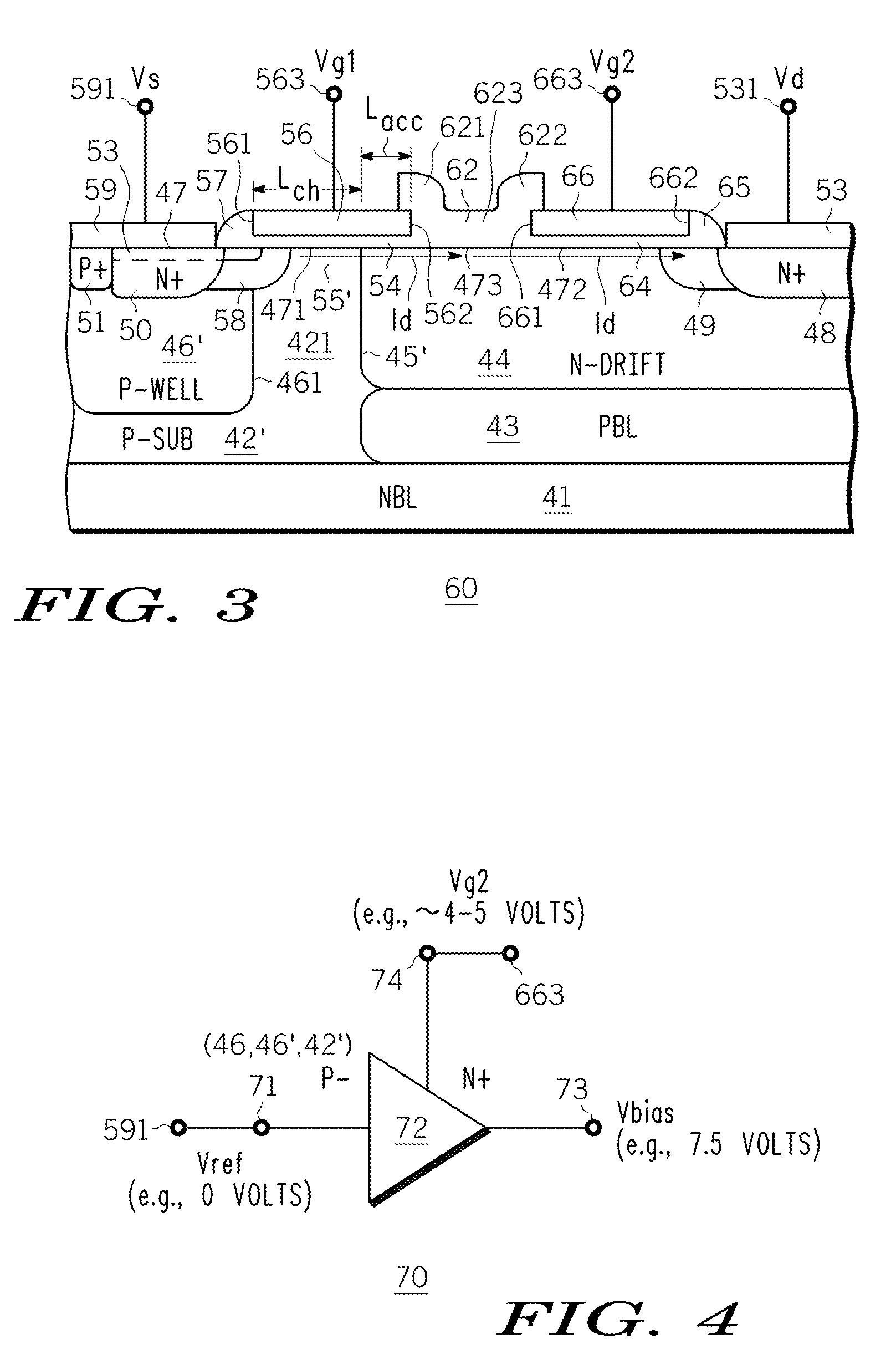
[0045] there is provided a semiconductor device, comprising, a semiconductor substrate of a first conductivity type and first dopant concentration and having a surface, a first well of the first conductivity type and second dopant concentration located in the substrate, a second well of a second, opposite, conductivity type and third dopant concentration located in the substrate, separated from or in contact with the first well and forming a PN junction with the first well or the substrate, which PN junction extends substantially to the surface, a third region of the second conductivity type and a fourth dopant concentration, located in the substrate, extending substantially to the surface and laterally separated from the first well, and adapted when biased to form a space charge region at least partly in the substrate or the first well or in a combination thereof, a first gate overlying a part of the first well or a part of the substrate between the first and second wells or both, ...

third embodiment

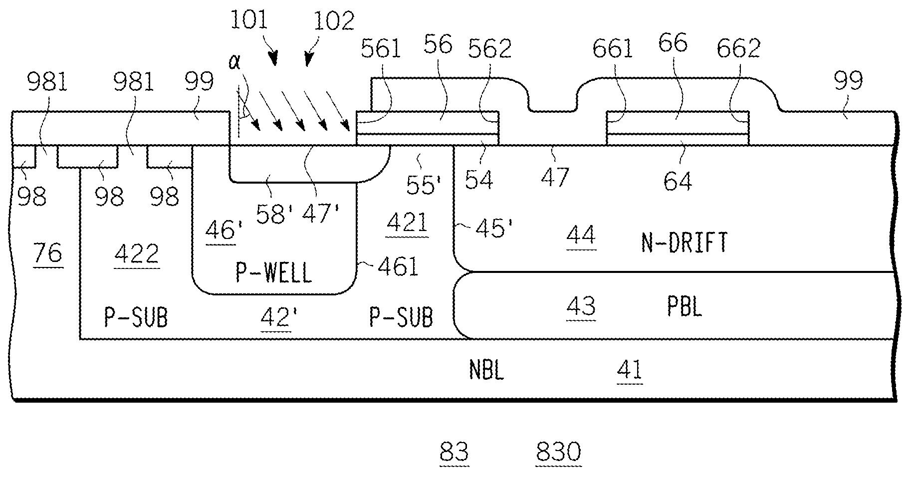
[0046] there is provided an LDMOS device, comprising, a semiconductor substrate of a first conductivity type and first concentration, having a principal surface, a source region of a second, opposite, conductivity type extending to the principal surface, a drain region of a second, opposite, conductivity type extending to the principal surface and spaced apart from the source region, a first gate, adapted to receive a control signal and located above a first portion of the principal surface proximate the source region, a second gate, adapted to receive a bias voltage Vg2 and located above the principal surface proximate the drain region and spaced apart from the first gate, a further region of the second conductivity type and further dopant concentration greater than the first concentration, located in the substrate and adapted to form a space charge region in the substrate when the further region receives a voltage Vbias, and a body contact coupled to the second gate for providing ...


PUM


Abstract

An N-channel device (40, 60) is described having a lightly doped substrate (42, 42′) in which adjacent or spaced-apart P (46, 46′) and N (44) wells are provided. A lateral isolation wall (76) surrounds at least a portion of the substrate (42, 42′) and is spaced apart from the wells (46, 46′, 44). A first gate (G1) (56) overlies the P (46) well or the substrate (42′) between the wells (46′, 44) or partly both. A second gate (G2) (66), spaced apart from G1 (56), overlies the N-well (44). A body contact (74) to the substrate (42, 42′) is spaced apart from the isolation wall (76) by a first distance (745) within the space charge region of the substrate (42, 42′) to isolation wall (76) PN junction. When the body contact (74) is connected to G2 (66), a predetermined static bias Vg2 is provided to G2 (66) depending upon the isolation wall bias (Vbias) and the first distance (745). The resulting device (40, 60) operates at higher voltage with lower Rdson and less HCI.

Description

FIELD OF THE INVENTION[0001]The present invention generally relates to semiconductor devices and methods for fabricating semiconductor devices, and more particularly relates to laterally diffused metal-oxide-semiconductor devices (LDMOS) employing dual gates, and methods therefore.BACKGROUND OF THE INVENTION[0002]Processing technologies and device structures for forming integrated circuits (ICs) are implemented by using a plurality of interconnected field effect transistors (FETs), also called metal oxide semiconductor field effect transistors (MOSFETs), or simply MOS transistors or devices. A well known sub-set of MOS transistors are referred to as laterally diffused metal oxide semiconductor (LDMOS) transistors or devices. Although the term “MOS device” properly refers to a device having a metal gate electrode and an oxide gate insulator, that term will be used throughout to refer to any semiconductor device that includes a conductive gate electrode (whether metal or not) that is ...

Claims


Application Information

Patent Timeline
IPC IPC(8): H01L21/04
CPCH01L21/26586H01L29/0692H01L29/0847H01L29/1045H01L29/7835H01L29/402H01L29/66537H01L29/66659H01L29/7831H01L29/1083
Inventor YANG, HONGNINGMACARY, VERONIQUE C.MIN, WON GIZUO, JIANG-KAI
Owner NORTH STAR INNOVATIONS
Why Eureka
Try Eureka