Ion beam treatment for the structural integrity of air-gap iii-nitride devices produced by the photoelectrochemical (PEC) etching

a technology of photoelectrochemical and air-gap iii, which is applied in the direction of basic electric elements, semiconductor devices, electrical apparatus, etc., can solve the problems of etch selectivity limitations, prior work, and etching bowing and warping of membrane layers, and achieve the effect of stiction of closely spaced membrane layers

Inactive Publication Date: 2008-07-31
RGT UNIV OF CALIFORNIA
View PDF7 Cites 38 Cited by
  • Summary
  • Abstract
  • Description
  • Claims
  • Application Information

AI Technical Summary

Benefits of technology

[0021]6) A suitable scheme to inspect the etch condition a

Problems solved by technology

The primary limitations to prior work has been (1) limitations in etch selectivity, (2) bowing and warping of the membranes due to inherent strain, and (3) stiction of closely space membrane layers (as in DBRs).
While air-gap DBR structures have been formed in other material systems, through simple, selective wet chemical etch processes (i.e

Method used


Image

  • Ion beam treatment for the structural integrity of air-gap iii-nitride devices produced by the photoelectrochemical (PEC) etching
  • Ion beam treatment for the structural integrity of air-gap iii-nitride devices produced by the photoelectrochemical (PEC) etching
  • Ion beam treatment for the structural integrity of air-gap iii-nitride devices produced by the photoelectrochemical (PEC) etching

Examples


Embodiment Construction

[0034]In the following description of the preferred embodiment, reference is made to the accompanying drawings which form a part hereof, and in which is shown by way of illustration a specific embodiment in which the invention may be practiced. It is to be understood that other embodiments may be utilized and structural changes may be made without departing from the scope of the present invention.

[0035]Overview

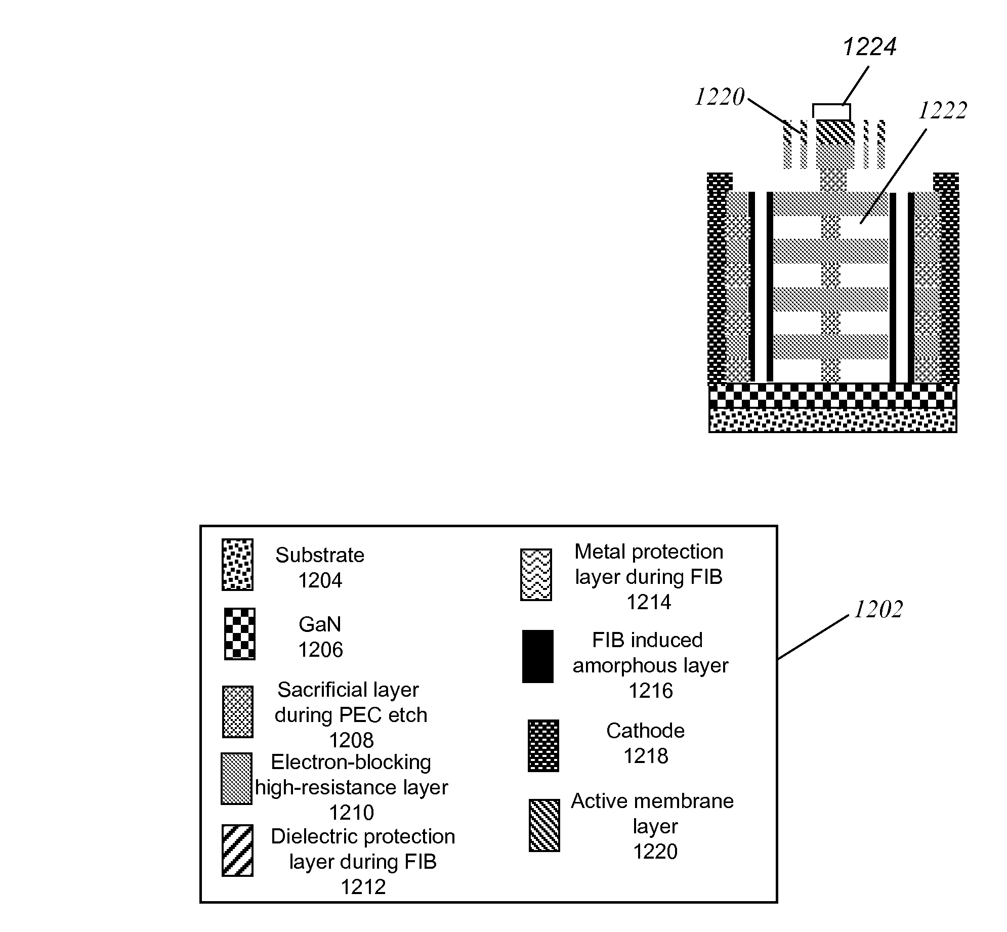
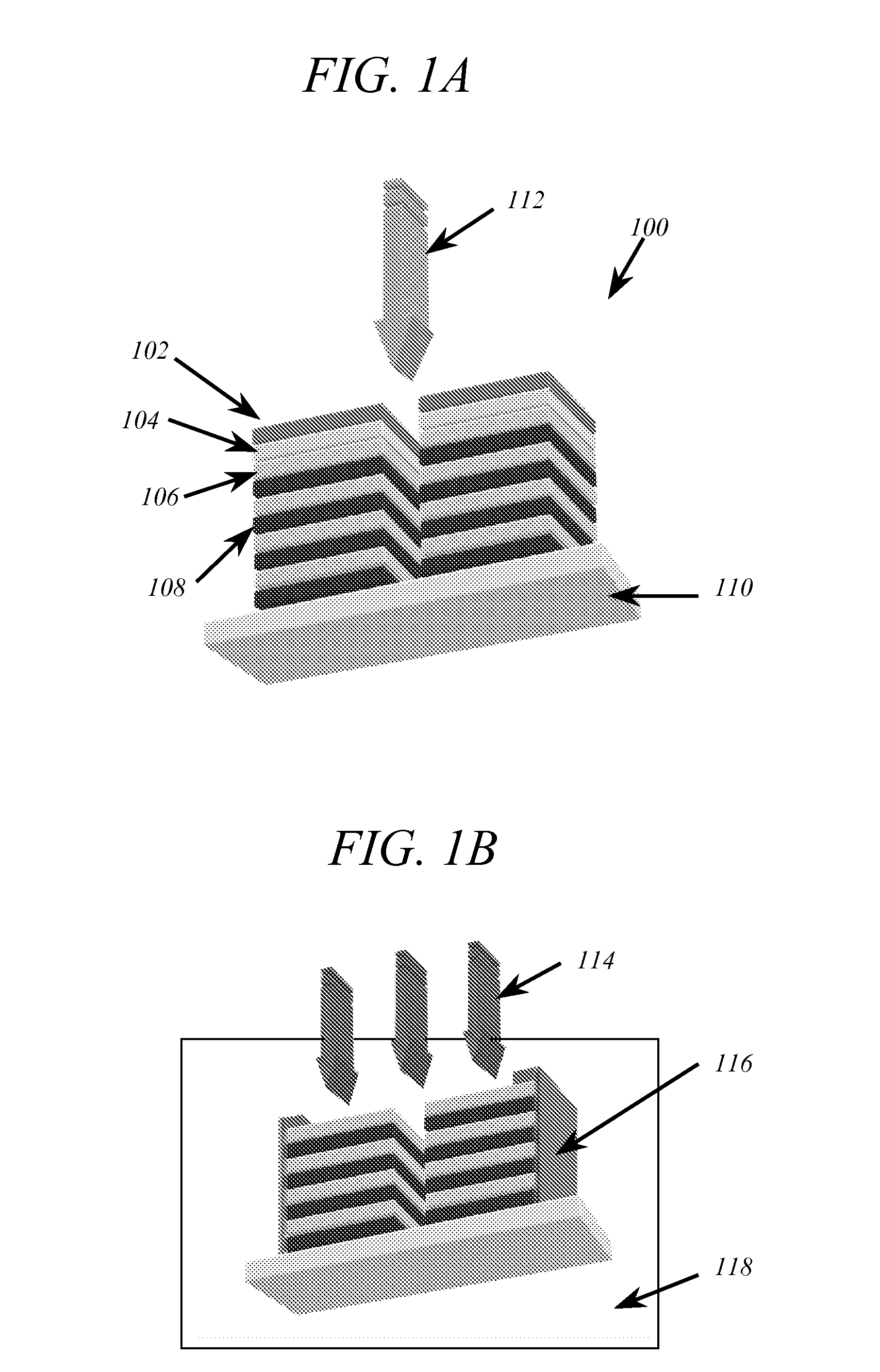
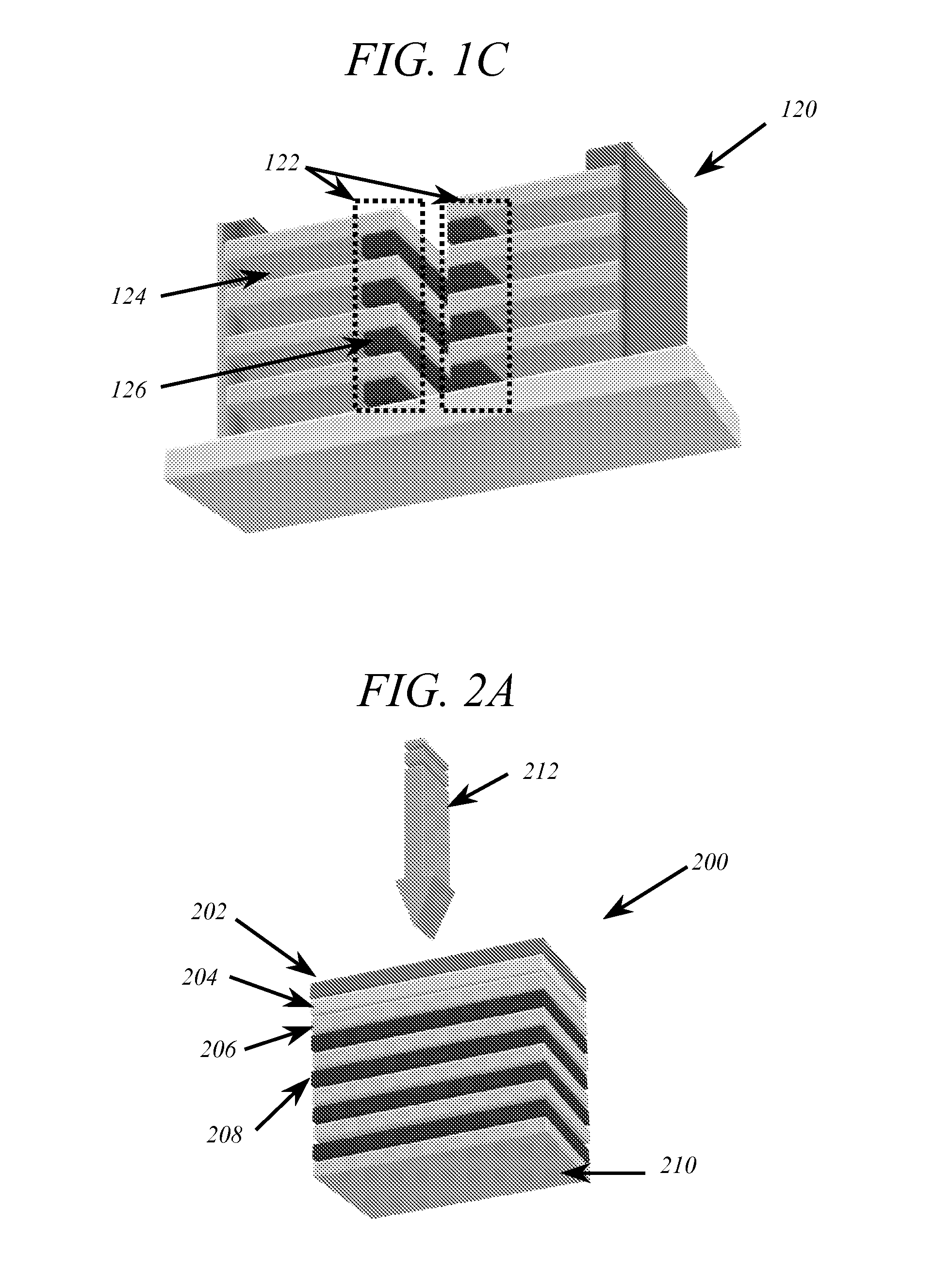
[0036]Advances in III-nitride processing have led to the formation of air-gap DBRs [1], high-quality microdisk lasers [2,3], and CAVET [4], and free-standing photonic crystal (PC) membrane nanocavities [5,6]. In the present invention, the unique control over the selective removal of embedded materials is obtained by a PEC wet-etching technique [7-16]. This selective wet etching can allow the larger index contrast between the air and the remaining material for higher index contrast in the DBRs, and therefore achievement of higher reflectivity with fewer mirror layers.

[0037]Comb...


PUM


Abstract

A method for ensuring the structural integrity of III-nitride opto-electronic or opto-mechanical air-gap nano-structured devices, comprising (a) performing ion beam implantation in a region of the III-nitride opto-electronic and opto-mechanical air-gap nano-structured device, wherein the milling significantly locally modifies a material property in the region to provide the structural integrity; and (b) performing a band-gap selective photo-electro-chemical (PEC) etch on the III-nitride opto-electronic and opto-mechanical air-gap nano-structured device. The method can be used to fabricate distributed Bragg reflectors or photonic crystals, for example. The method also comprises the suitable design of distributed Bragg reflector (DBR) structures for the PEC etching and the ion-beam treatment, the suitable design of photonic crystal distributed Bragg reflector (PCDBR) structures for PEC etching and the ion-beam treatment, the suitable placement of protection layers to prevent the ion-beam damage to optical activity and PEC etch selectivity, and a suitable annealing treatment for curing the material quality after the ion-beam treatment.

Description

CROSS-REFERENCE TO RELATED APPLICATIONS[0001]This application claims the benefit under 35 U.S.C. Section 119(e) of the following co-pending and commonly-assigned U.S. provisional patent application:[0002]Provisional Application Ser. No. 60 / 866,027, filed Nov. 15, 2006, by Evelyn L. Hu, Shuji Nakamura, Yong Seok Choi, Rajat Sharma, and Chio-Fu Wang, entitled “ION BEAM TREATMENT FOR THE STRUCTURAL INTEGRITY OF AIR-GAP III-NITRIDE DEVICES PRODUCED BY PHOTOELECTROCHEMICAL (PEC) ETCHING,” attorneys' docket number 30794.201-US-P1 (2007-161-1);[0003]which application is incorporated by reference herein.[0004]This application is related to the following co-pending and commonly-assigned applications:[0005]U.S. Utility application Ser. No. 11 / 263,314, filed on Oct. 31, 2005, by Evelyn L. Hu, Shuji Nakamura, Elaine D. Haberer, and Rajat Sharma, entitled “CONTROL OF PHOTOELECTROCHEMICAL (PEC) ETCHING BY MODIFICATION OF THE LOCAL ELECTROCHEMICAL POTENTIAL OF THE SEMICONDUCTOR STRUCTURE RELATIVE ...

Claims


Application Information

Patent Timeline
IPC IPC(8): H01L21/302
CPCH01L33/0075H01L33/10H01L33/0095
Inventor HU, EVELYN L.NAKAMURA, SHUJICHOI, YONG SEOKSHARMA, RAJATWANG, CHIOU-FU
Owner RGT UNIV OF CALIFORNIA
Why Eureka
Try Eureka