Integrated circuit design for reducing coupling between wires of an electronic circuit

Inactive Publication Date: 2008-07-31
GLOBALFOUNDRIES INC
23 Cites 4 Cited by

AI-Extracted Technical Summary

Problems solved by technology

Making electronics smaller and smaller raises new challenges in manufacturing CPUs and ASICs.
Designing modern electrical circuits such as CPUs and ASICs with wire dimensions of 130 nm and below has become increasingly difficult due to shrinking distance rules (“wire pitch”) which cause capacitive coupling between proximate wires.
In any case this can cause a digital system to fail because wrong signal values may be propagated.
The drawbacks are that the logic changes require the design infrastructure to support the ability to modify cells on routed designs.
I...

Method used

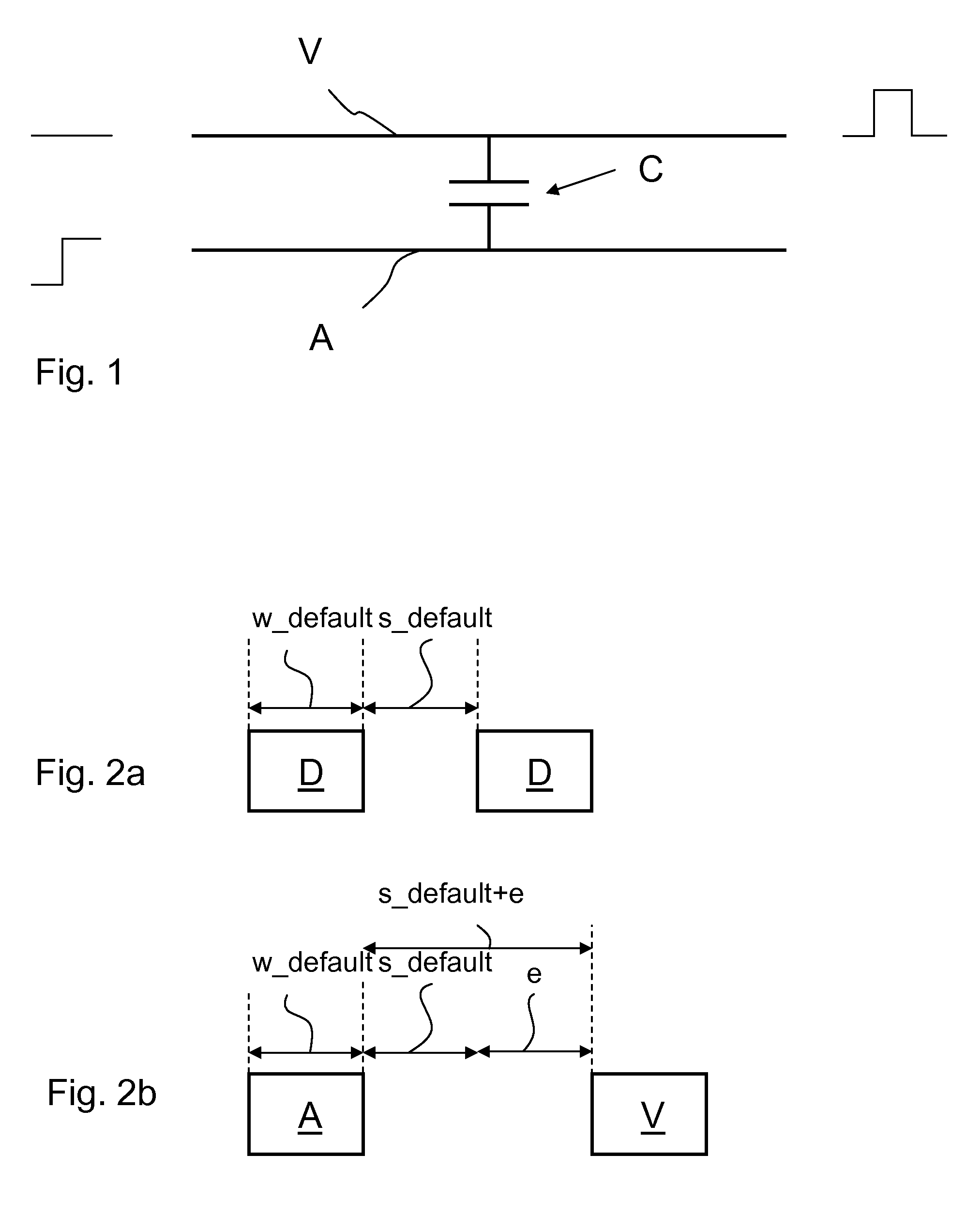
[0102]The matrices of both tables in FIGS. 3 and 4, respectively, can be adapted to save additional wiring resources. Another improvement, additionally or alternatively, can be to add a weighing function to timing critical nets to avoid detours in important signals.
[0120]A computer processing system suitable for storing and/or executing program code will include at least o...

Benefits of technology

[0038]Additional types of victim and aggressor nets can be included. The distance and/or wire widths rules can be adapted to save additional wiring resources.
[0039]To avoid detours on important signals, it is possible to apply a...

Abstract

A design structure for reducing coupling between wires of an electronic circuit is proposed, wherein sets of nets are classified according to their coupling characteristics, and spacing between wires assigned to the sets of nets is chosen according to the coupling characteristics.

Application Domain

Computer aided designSoftware simulation/interpretation/emulation +2

Technology Topic

Integrated circuitElectronic circuit +3

Image

  • Integrated circuit design for reducing coupling between wires of an electronic circuit
  • Integrated circuit design for reducing coupling between wires of an electronic circuit
  • Integrated circuit design for reducing coupling between wires of an electronic circuit

Examples

  • Experimental program(1)

Example

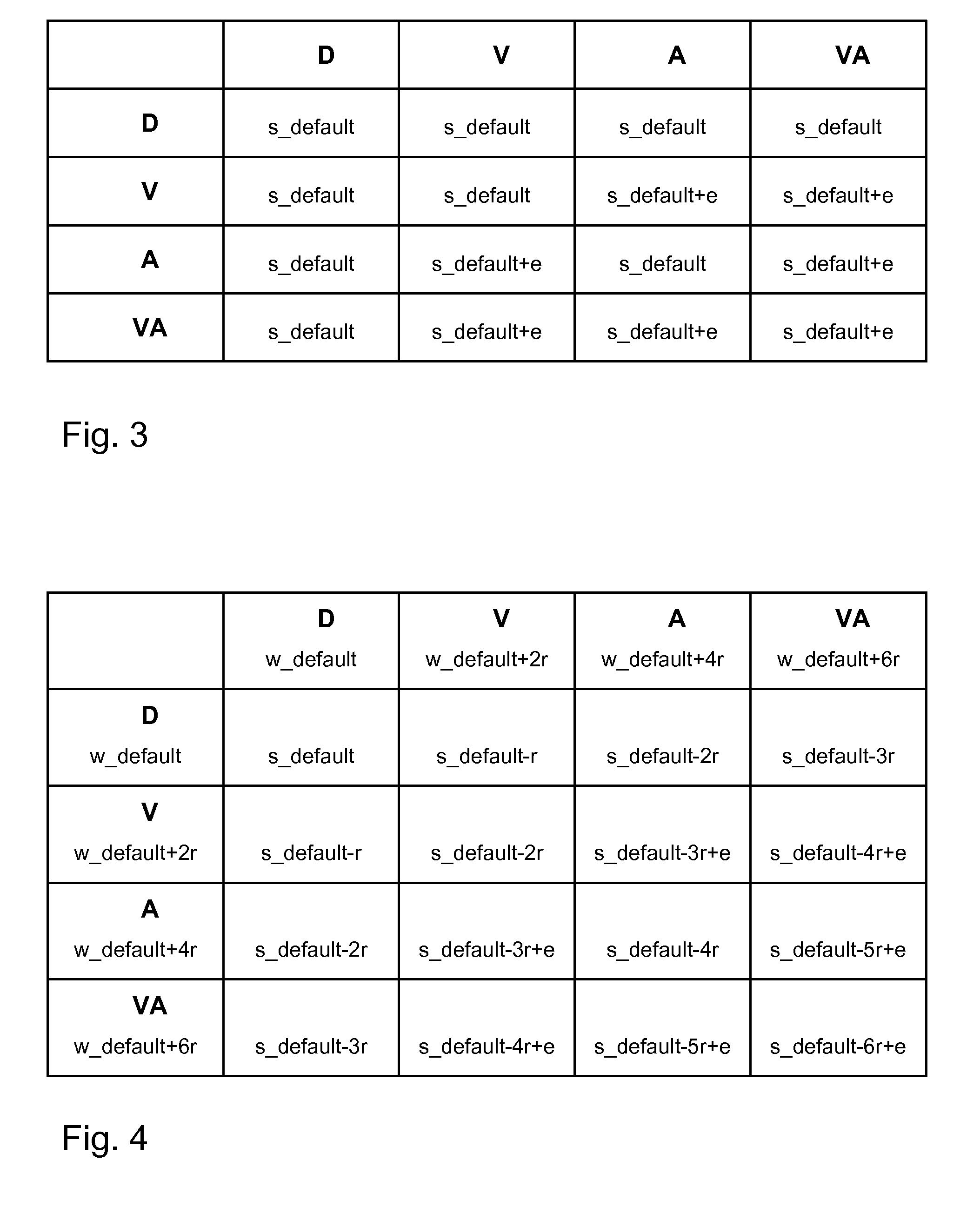
[0091]A table can be generated similar to the table in FIG. 3 for the first embodiment, as is depicted by the table in FIG. 4.
[0092]Again, a first distance rule between a first wire and a second proximate wire is applied, unless [0093] the first wire is a victim wire V and the second wire is an aggressor wire A or a victim-aggressor wire VA, or [0094] the first wire is an aggressor wire A and the second wire is a victim-aggressor wire VA, or [0095] the first wire is a victim-aggressor wire VA and the second wire is a victim wire V or an aggressor wire A or a victim-aggressor wire VA,
where for these cases a second distance rule is applied.
[0096]With the first distance rule a wire spacing s3 is applied, which is decreasing in units of the router resolution, starting form the default spacing s_default between two proximate default wires D. With the second distance rule an additional spacing e is added to the first wire spacing s3.
[0097]With the first wire a default wire D, the spacing to a proximate victim wire is s_default−r, the spacing to a proximate aggressor wire A is s_default−2r and to a proximate victim-aggressor wire VA is s_default−3r.
[0098]If the first wire is a victim wire V and the proximate wire is a default wire D, the spacing is s_default−r, with the proximate wire being a victim wire V, the spacing is s_default−2r, with the proximate wire an aggressor wire A, the spacing is s_default−3r+e, and with the proximate wire a victim-aggressor wire VA, the spacing is s_default−4r+e.
[0099]If the first wire is an aggressor wire A and the proximate wire is a default wire D, the spacing is s_default−2r, with the proximate wire a victim wire V, the spacing is s_default−3r+e, with the proximate wire an aggressor wire A, the spacing is s_default−4r, with the proximate wire a victim-aggressor wire VA, the spacing is s_default−5r+e.
[0100]If the first wire is a victim-aggressor wire VA and the proximate wire is a default wire D, the spacing is s_default−3r, with the proximate wire being a victim wire V, the spacing is s_default−4r+e, with the proximate wire an aggressor wire A, the spacing is s_default−5r+e, and with the proximate wire a victim-aggressor wire VA, the spacing is s_default−6r+e.
[0101]The approaches described in the embodiments can be modified to include additional classes of victim and aggressor nets and/or different wire widths.
[0102]The matrices of both tables in FIGS. 3 and 4, respectively, can be adapted to save additional wiring resources. Another improvement, additionally or alternatively, can be to add a weighing function to timing critical nets to avoid detours in important signals.
[0103]The IC design is characterized by the steps of [0104] defining sets of nets of different kinds, especially default nets, victim nets, aggressor nets, and victim-aggressor nets, [0105] perform global routing of the electronic circuit, for each net yielding an area which is a small subset of the entire chip area, where local routing can be performed, [0106] run a coupling analysis, in order to verify or falsify the coupling characteristics of the nets, [0107] assign wire types V, A, AV, D to the kinds of nets, [0108] perform local routing, in order to actually embed the wires and thus determine their location, [0109] run a coupling analysis based on the local routing results, [0110] assign wire types V, A, AV, D to the kinds of nets, [0111] rip-up and reroute possible new wire types V, A, AV, D, found in the coupling analysis, and allowing rip-up of others, [0112] repeat routing and assigning steps if necessary, [0113] reset wire widths to original widths if necessary, [0114] return from routing.
[0115]FIG. 5 shows a block diagram of an example design flow 500. Design flow 500 may vary depending on the type of integrated circuit (IC) being designed. For example, a design flow 500 for building an application specific IC (ASIC) may differ from a design flow 500 for designing a standard component. Design structure 520 is preferably an input to a design process 510 and may come from an IP provider, a core developer, or other design company or may be generated by the operator of the design flow, or from other sources. Design structure 520 comprises a circuit in the form of schematics or HDL, a hardware-description language (e.g., Verilog, VHDL, C, etc.). Design structure 520 may be contained on one or more machine readable medium. For example, design structure 520 may be a text file or a graphical representation of the circuit. Design process 510 preferably synthesizes (or translates) the circuit into a netlist 580, where netlist 580 is, for example, a list of wires, transistors, logic gates, control circuits, I/O, models, etc. that describes the connections to other elements and circuits in an integrated circuit design and recorded on at least one of machine readable medium. This may be an iterative process in which netlist 580 is resynthesized one or more times depending on design specifications and parameters for the circuit.
[0116]Design process 510 may include using a variety of inputs; for example, inputs from library elements 530 which may house a set of commonly used elements, circuits, and devices, including models, layouts, and symbolic representations, for a given manufacturing technology (e.g., different technology nodes, 32 nm, 45 nm, 50 nm, etc.), design specifications 540, characterization data 550, verification data 560, design rules 570, and test data files 585 (which may include test patterns and other testing information). Design process 510 may further include, for example, standard circuit design processes such as timing analysis, verification, design rule checking, place and route operations, etc. One of ordinary skill in the art of integrated circuit design can appreciate the extent of possible electronic design automation tools and applications used in design process 510 without deviating from the scope and spirit of the invention. The design structure of the invention is not limited to any specific design flow.
[0117]Ultimately, design process 510 preferably translates the circuit, along with the rest of the integrated circuit design (if applicable), into a final design structure 590 (e.g., information stored in a GDS storage medium). Final design structure 590 may comprise information such as, for example, test data files, design content files, manufacturing data, layout parameters, wires, levels of metal, vias, shapes, test data, data for routing through the manufacturing line, and any other data required by a semiconductor manufacturer to produce the circuit. Final design structure 590 may then proceed to a stage 595 where, for example, final design structure 590: proceeds to tape-out, is released to manufacturing, is sent to another design house or is sent back to the customer.
[0118]The invention can take the form of an entirely hardware embodiment, an entirely software embodiment or an embodiment containing both hardware and software elements. In an embodiment, the invention is implemented in software, which includes but is not limited to firmware, resident software, microcode, etc.
[0119]Furthermore, the invention can take the form of a computer program product accessible from a computer-usable or computer-readable medium providing program code for use by or in connection with a computer or any instruction execution system. For the purposes of this description, a computer-usable or computer-readable medium can be any apparatus that can contain, store, communicate, propagate, or transport the program for use by or in connection with the instruction execution system, apparatus, or device.
[0120]A computer processing system suitable for storing and/or executing program code will include at least one processor coupled directly or indirectly to memory elements through a system bus. The memory elements can include local memory employed during actual execution of the program code, bulk storage, and cache memories which provide temporary storage of at least some program code in order to reduce the number of times code must be retrieved from bulk storage during execution.
[0121]While a particular embodiment has been shown and described, various modifications of the present invention will be apparent to those skilled in the art.

PUM

no PUM

Description & Claims & Application Information

We can also present the details of the Description, Claims and Application information to help users get a comprehensive understanding of the technical details of the patent, such as background art, summary of invention, brief description of drawings, description of embodiments, and other original content. On the other hand, users can also determine the specific scope of protection of the technology through the list of claims; as well as understand the changes in the life cycle of the technology with the presentation of the patent timeline. Login to view more.
Why Eureka
Try Eureka