Method of manufacturing printed circuit board

a manufacturing method and printed circuit board technology, applied in the direction of printed circuits, printed circuit aspects, stress/warp reduction of printed circuits, etc., can solve the problems of increasing the specification of the substrate proportional to the increase in the density of the semiconductor, which is almost impossible to achieve in practice, and many process defects. to achieve the effect of minimizing the warping

Inactive Publication Date: 2008-08-07
SAMSUNG ELECTRO MECHANICS CO LTD
View PDF5 Cites 6 Cited by
  • Summary
  • Abstract
  • Description
  • Claims
  • Application Information

AI Technical Summary

Benefits of technology

[0011]Leading to the present invention, intensive and extensive research into methods of manufacturing PCBs, aiming to solve the problems encountered in the related art, resulted in the finding that a dummy metal frame enclosing the outer periphery of a product part may be formed, thereby simultaneously assuring the rigidity of a PCB and minimizing the warping thereof, thanks to the dummy metal frame left in place on a finished product.
[0012]Accordingly, the present invention provides a method of manufacturing a PCB for flip chip mounting, having a coreless structure for minimizing the impedance of a substrate for mounting a semiconductor.
[0013]In addition, the present invention provides a method of manufacturing a PCB, which facilitates the mounting of a semiconductor on a coreless PCB.
[0014]In addition, the present invention provides a method of manufacturing a PCB, which is capable of assuring the rigidity of the PCB and minimizing the warping thereof in the formation of circuits.

Problems solved by technology

Although flip chip mounting requires a highly reliable substrate having high density, an increase in the specification of the substrate in proportion to the increase in the density of the semiconductor is almost impossible to achieve in practice.
However, high performance of semiconductors results in heat generation, which is regarded as a big mechanical problem.
However, in the case where a coreless substrate, such as an ultra-thin substrate, is manufactured using the conventional method, the following two problems are incurred.
First, when a substrate having low rigidity without a base plate is formed into a built-up structure by repeating the formation of insulating layers, interlayer connection processing, and the formation of circuits using conventional equipment, many process defects, including the dropping of the substrate from a horizontal conveying device, interruption of conveyance, overlapping of substrates in basket-type treatment, and damage to the substrate during handling, are generated.
Second, attributable to the substrate having low rigidity without the base plate, a finished substrate may easily warp, thus making it impossible to fulfill the demands of consumers.

Method used


Image

  • Method of manufacturing printed circuit board
  • Method of manufacturing printed circuit board
  • Method of manufacturing printed circuit board

Examples


Embodiment Construction

[0024]Hereinafter, a detailed description will be given of the present invention, with reference to the appended drawings.

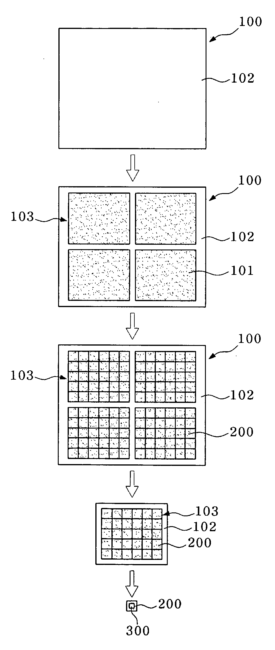
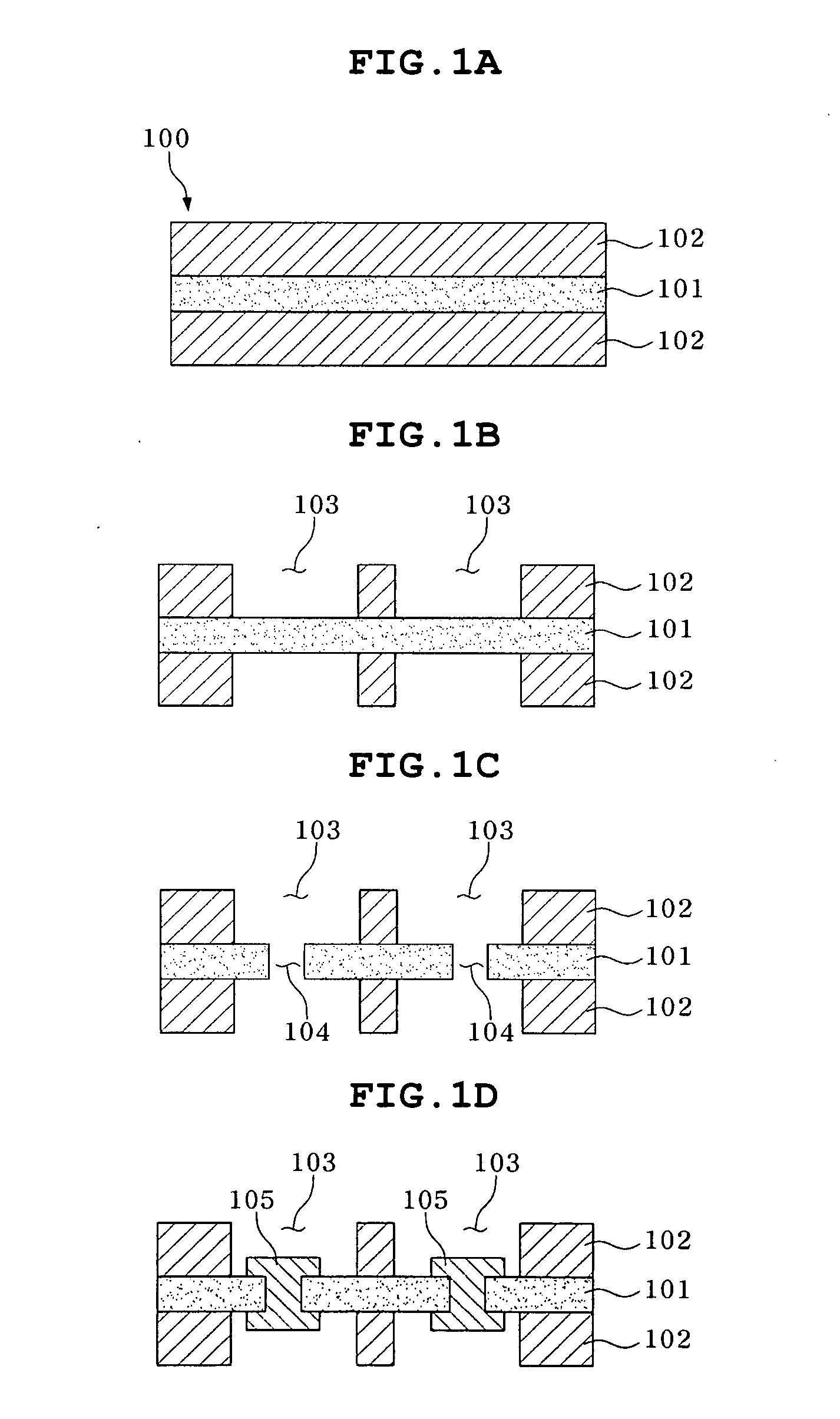
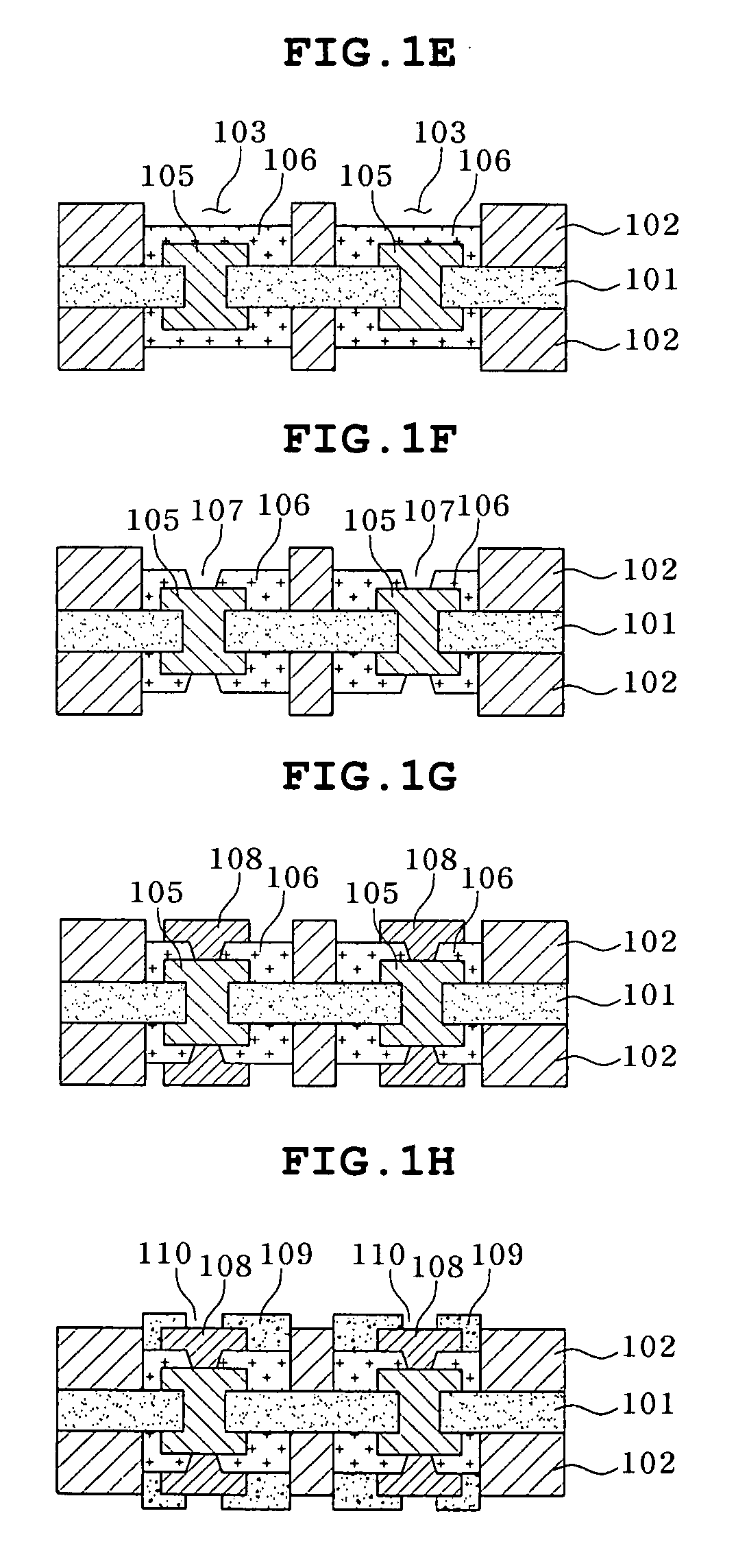
[0025]FIGS. 1A to 1J and FIG. 2 schematically and sequentially illustrate the process of manufacturing a PCB according to the present invention.

[0026]According to the present invention, a work substrate 100, having a resin substrate 101 and metal plates 102 having rigidity equal to or higher than 100 GPa on both surfaces thereof, is prepared (FIG. 1A and the first figure of FIG. 2). The type and thickness of the resin substrate 101 are not particularly limited so long as they are typical in the art. In the present invention, even when an ultra-thin substrate having a thickness less than or equal to 0.4 mm is used, it is possible to assure the rigidity of a PCB and minimize the warping thereof, and thus the above substrate is compatible with conventional flip chip mounting lines. The use of metal plates 102, having rigidity equal to or higher than 100 GPa, and pre...


PUM

PropertyMeasurementUnit
thicknessaaaaaaaaaa
thicknessaaaaaaaaaa
rigidityaaaaaaaaaa

Abstract

This invention relates to a method of manufacturing a printed circuit board, in which a dummy metal frame enclosing the outer periphery of a product part is formed, thus simultaneously assuring the rigidity of the printed circuit board and minimizing the warping thereof thanks to the dummy metal frame left in place on a finished product, thereby realizing a structure compatible with conventional flip chip mounting lines.

Description

CROSS REFERENCE TO RELATED APPLICATION[0001]This application claims the benefit of Korean Patent Application No. 10-2007-0012745, filed on Feb. 7, 2007, entitled “Method for manufacturing printed circuit board”, which is hereby incorporated by reference in its entirety into this application.BACKGROUND OF THE INVENTION[0002]1. Field of the Invention[0003]The present invention relates, in general, to a method of manufacturing a printed circuit board (PCB). More particularly, the present invention relates to a method of manufacturing a PCB, in which a dummy metal frame enclosing the outer periphery of a product part is left in place until the completion of a product, so that, during the formation of circuits, the rigidity of the PCB is assured and the generation of defects due to warping is minimized.[0004]2. Description of the Related Art[0005]In order for technology to keep up with the trend of increasing the signal transmission speed and the density of semiconductor chips, the deman...

Claims


Application Information

Patent Timeline
Patent Type & Authority Applications(United States)
IPC IPC(8): H05K3/22
CPCH05K1/0271H05K3/0052H05K2201/09781H05K2203/0169Y10T29/49165Y10T29/49128Y10T29/49155Y10T29/49126Y10T29/49147H05K3/46
Inventor HAZE, TAKAYUKI
Owner SAMSUNG ELECTRO MECHANICS CO LTD
Why Eureka
Try Eureka