Microelectromechanical system package and the method for manufacturing the same

a micro-electromechanical and system package technology, applied in the field of wafer-level micro-electromechanical system package, can solve the problems of difficult mass production of such packages b>100/b> and its application is quite limited, and achieve the effect of reducing the thickness of the packag

Active Publication Date: 2008-08-07
ADVANCED SEMICON ENG INC
View PDF24 Cites 18 Cited by
  • Summary
  • Abstract
  • Description
  • Claims
  • Application Information

AI Technical Summary

Benefits of technology

[0008]It is an object of the present invention to provide a method for manufacturing microelectromechanical system packages that uses a wafer as a cover to protect the microelectromechanical system chips in the packages and the thickness of the package can therefore be reduced.

Problems solved by technology

However, the mass production of such packages 100 is difficult.
Moreover, the package 100 has a large profile and therefore its application is quite limited.

Method used


Image

  • Microelectromechanical system package and the method for manufacturing the same
  • Microelectromechanical system package and the method for manufacturing the same
  • Microelectromechanical system package and the method for manufacturing the same

Examples


Embodiment Construction

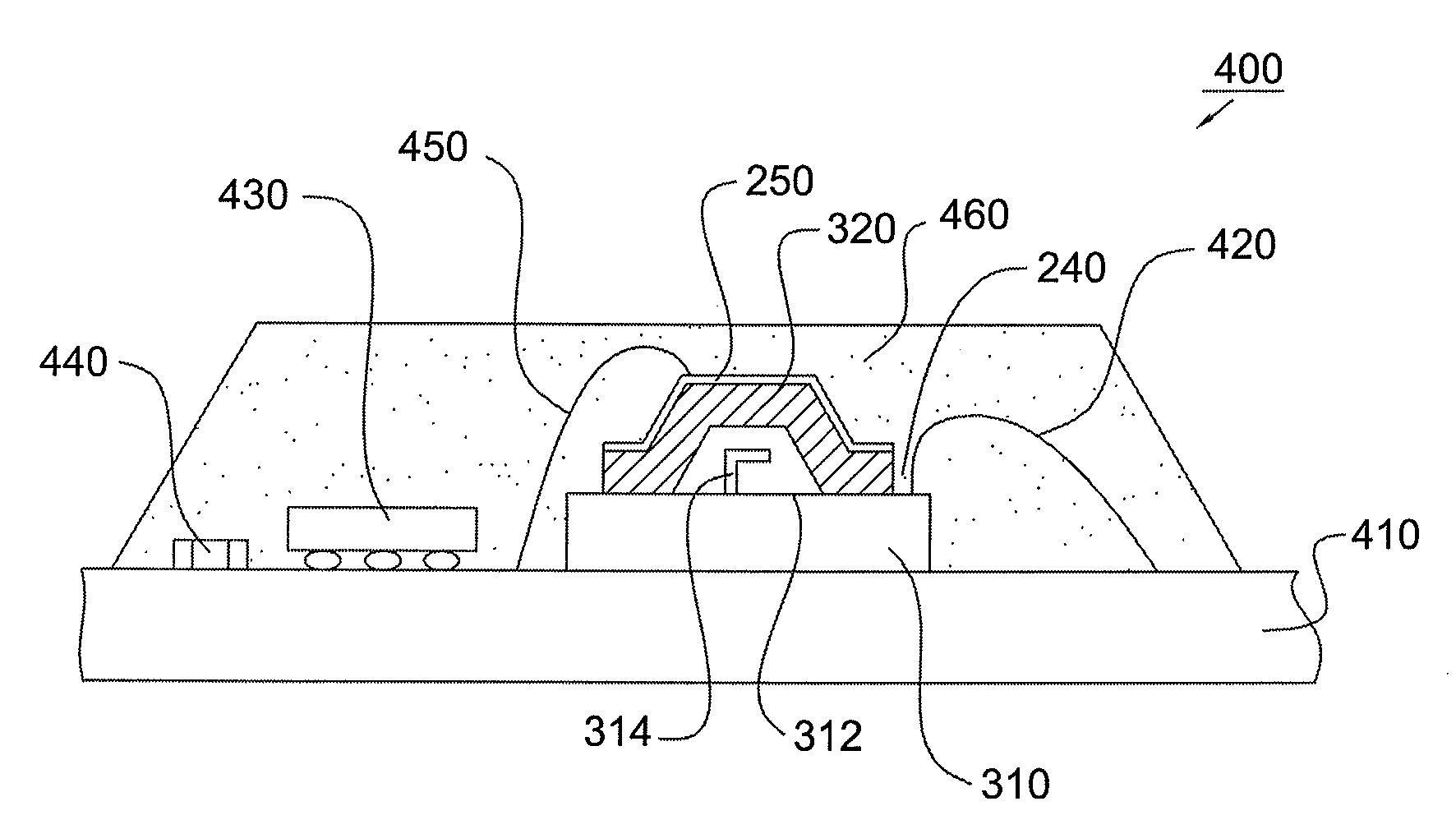
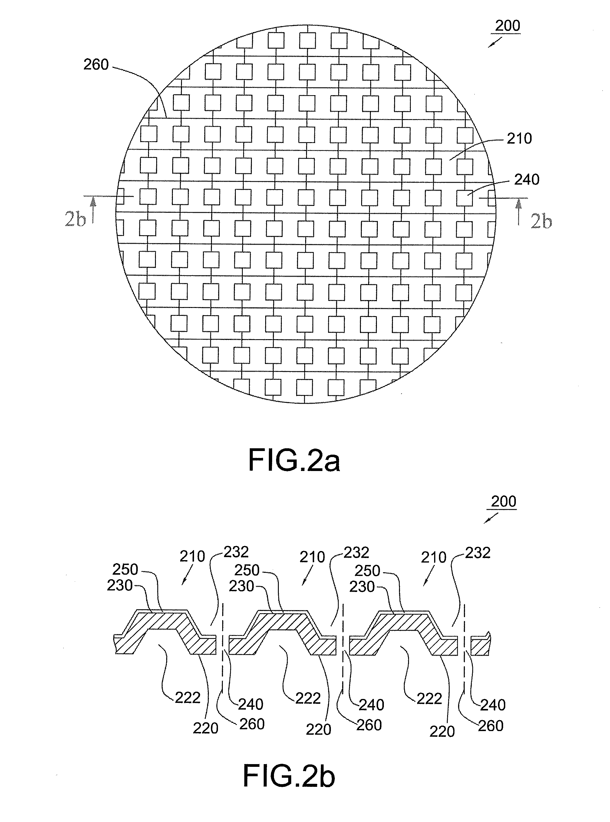
[0016]Referring to FIGS. 2a and 2b, the method for manufacturing microelectromechanical system (MEMS) chips according to the present invention is first to provide a cover 200, such as a silicon wafer. The cover 200 defines a plurality of units 210 and these units 210 are separated from each other by a plurality of scribe streets 260. The lower surface 220 of the cover 200 is etched to form a plurality of wedge-shaped cavities 222 in the units 210, respectively. The upper surface 230 of the cover 200 is also etched to form a plurality of cavities 232, wherein each of the cavities 232 is formed across one of the scribe streets 260 between an adjacent pair of the units 210. A plurality of through openings 240 is formed on the bottoms of the cavities 232 and penetrates to the lower surface 220 of the cover 200, respectively, and each of the openings 240 is located across one of the scribe streets 260 between an adjacent pair of the units 210. A layer of metal 250, such as a copper (Cu) ...


PUM


Abstract

A method for manufacturing a microelectromechanical system package is provided. A plurality of cavities is first formed on the upper and lower surfaces of a silicon wafer. Next, the lower surface of the silicon wafer is bonded to the microelectromechanical system wafer in such a manner that the active areas of the chips on the microelectromechanical system wafer are received in the cavities on the lower surface of the silicon wafer, respectively. Finally, the structure assembly of the two wafers is singulated along the scribe streets to form individual microelectromechanical system chips whose active areas are covered by the cavities. These microelectromechanical system chips together with other components can be mounted to chip carriers to form microelectromechanical system packages.

Description

CROSS REFERENCE TO RELATED APPLICATION [0001]This application claims the priority benefit of Taiwan Patent Application Serial Number 096104252 filed Feb. 6, 2007, the full disclosure of which is incorporated herein by reference.BACKGROUND OF THE INVENTION [0002]1. Field of the Invention[0003]The invention relates to a microelectromechanical system package and the method for manufacturing the same, and more particularly, to a wafer-level microelectromechanical system package and the method for manufacturing the same.[0004]2. Description of the Related Art[0005]Referring to FIG. 1, a conventional microelectromechanical system package 100 includes a substrate 110 and a microelectromechanical system (MEMS) device 120 disposed on the substrate 110. A cover 130 is disposed on the substrate 110 to cover the MEMS device 120. A peripheral edge of the cover 130 is electrically connected to the substrate 110 by a conductive adhesive, solder, or the like 140. The cover 130 includes an outer cup...

Claims


Application Information

Patent Timeline
Patent Type & Authority Applications(United States)
IPC IPC(8): H01L23/495H01L21/00
CPCB81C1/00269B81C2203/0118H01L2924/1461H01L2924/3025H01L2924/10253H01L2924/19105H01L2224/48091H01L2224/16225H01L2924/00014H01L2924/00H01L2924/00011H01L2224/0401
Inventor WANG, MENG JEN
Owner ADVANCED SEMICON ENG INC
Why Eureka
Try Eureka