Control of dry clean process in wafer processing

a technology of dry cleaning and wafers, applied in the direction of cleaning using liquids, cleaning processes and equipment, etc., can solve the problems of undesirable drift, inconsistent or inadequate cleaning process, and drift of the state of the chamber, so as to increase the effectiveness of the cleaning process

Inactive Publication Date: 2008-08-14
IBM CORP
View PDF14 Cites 3 Cited by
  • Summary
  • Abstract
  • Description
  • Claims
  • Application Information

AI Technical Summary

Benefits of technology

[0006]In view of the foregoing, an embodiment of the invention provides a method of cleaning an etch chamber. The method is “wafer-less” because all wafers are removed from the etch chamber before the cleaning process begins. After the wafer is removed, the invention varies the capacitance applied to radio frequency components of the chuck that is within the etch chamber (varies impedance of the chuck) so as to cause electric field lines within the etch chamber to terminate (bend) away from the ch

Problems solved by technology

Commonly, the cleaning process is inconsistent or inadequate, which changes from run to run.
This results in drift of the state of the chamber and in an undesirable drift of the results of product wafer processing.
Undesirable high drift over time leads to significant deterioration in chamber output performance calling for drastic procedures including frequent wet-cleans and extended duration dry-cleans.
Th

Method used


Image

  • Control of dry clean process in wafer processing
  • Control of dry clean process in wafer processing

Examples


Embodiment Construction

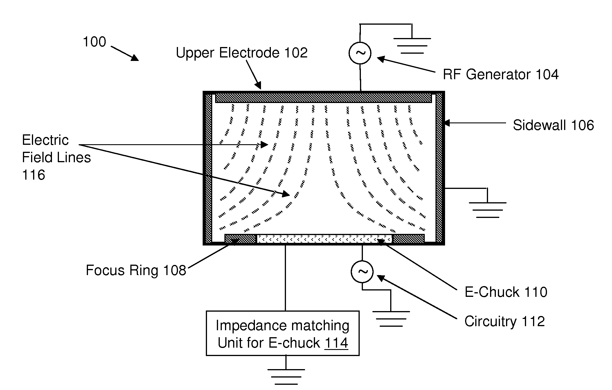
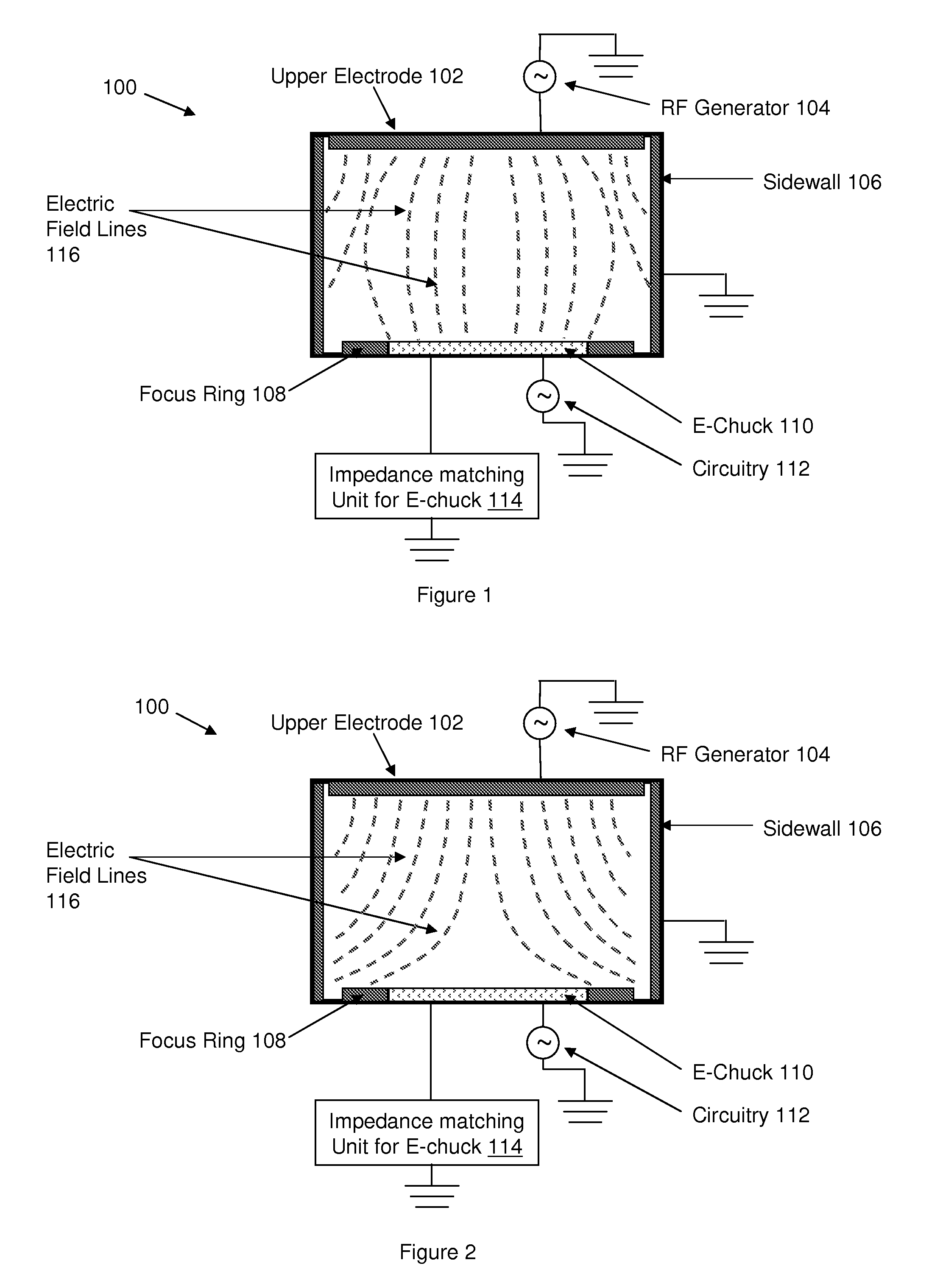
[0011]The embodiments of the invention and the various features and advantageous details thereof are explained more fully with reference to the non-limiting embodiments that are illustrated in the accompanying drawings and detailed in the following description. It should be noted that the features illustrated in the drawings are not necessarily drawn to scale. Descriptions of well-known components and processing techniques are omitted so as to not unnecessarily obscure the embodiments of the invention. The examples used herein are intended merely to facilitate an understanding of ways in which the embodiments of the invention may be practiced and to further enable those of skill in the art to practice the embodiments of the invention. Accordingly, the examples should not be construed as limiting the scope of the embodiments of the invention.

[0012]As mentioned above, inconsistencies in the cleaning of a semiconductor wafer etching chamber tends to produce inconsistent output. Such in...


PUM


Abstract

A “wafer-less” etch chamber cleaning method varies the capacitance applied to radio frequency components of the chuck that is within the etch chamber (varies impedance of the chuck) so as to cause electric field lines within the etch chamber to terminate (bend) away from the chuck. Then the etch chamber can be cleaned using a very aggressive etch chemistry (e.g., NF3) that would otherwise damage the chuck; however, the electric field lines protect the chuck from the etch chemistry. The capacitance is varied according to a pre-established model. Further, the process evaluates the effectiveness of the pre-established model to produce feedback and constantly adjusts the pre-established model to increase the effectiveness of the cleaning process (according to the feedback).

Description

BACKGROUND[0001]1. Field of the Invention[0002]The embodiments of the invention generally relate to semiconductor wafer processing, and, more particularly to processes that clean the dry etching chamber used in semiconductor wafer processing.[0003]2. Description of the Related Art[0004]During semiconductor wafer processing it is common to etch the wafers in etch chambers so as to selectively remove certain materials. In order to obtain good critical dimension (CD) control for critical etch applications (such as gate etch) it is crucial that the etch chamber be returned to the same or at least some predictable state after every product wafer is processed.[0005]The conventional methods perform dry (plasma) cleaning of the etch chamber after every product wafer is run. Commonly, the cleaning process is inconsistent or inadequate, which changes from run to run. This results in drift of the state of the chamber and in an undesirable drift of the results of product wafer processing. Undes...

Claims


Application Information

Patent Timeline
IPC IPC(8): B08B6/00
CPCH01L21/67028H01L21/6833H01L21/67051
Inventor RANADE, RAJIV M.KULKARNI, SUBHASH B.KROGH, OLEPATEL, SUKESH
Owner IBM CORP
Why Eureka
Try Eureka