Non-Volatile Magnetic Memory Element with Graded Layer

a magnetic memory element and non-volatile technology, applied in the field of non-volatile magnetic memory, can solve the problems of high power dissipation, large physical size, access latency, etc., and achieve the effect of reducing the switching current in the magnetic memory and high memory capacity

Active Publication Date: 2008-08-14
AVALANCHE TECH
View PDF99 Cites 81 Cited by
  • Summary
  • Abstract
  • Description
  • Claims
  • Application Information

AI Technical Summary

Benefits of technology

[0013]To overcome the limitations in the prior art described above, and to overcome other limitations that will become apparent upon reading and understanding the present specification, the present invention discloses a method and a corresponding structure for a non-volatile magnetic storage memory device that is based on current-induced-magnetization-switching having reduced switching current in the magnetic memory and high memory capacity.

Problems solved by technology

Though widely used and commonly accepted, such media suffer from a variety of deficiencies, such as access latency, higher power dissipation, large physical size and inability to withstand any physical shock.
Other dominant storage devices are dynamic random access memory (DRAM) and static RAM (SRAM) which are volatile and very costly but have fast random read / write access time.
Although NAND-based flash memory is more costly than HDD's, it has replaced magnetic hard drives in many applications such as digital cameras, MP3-players, cell phones, and hand held multimedia devices due, at least in part, to its characteristic of being able to retain data even when power is disconnected.
However, as memory dimension requirements are dictating decreased sizes, scalability is becoming an issue because the designs of NAND-based Flash memory and DRAM memory are becoming difficult to scale with smaller dimensions.
For example, NAND-based flash memory has issues related to capacitive coupling, few electrons / bit, poor error-rate performance and reduced reliability due to decreased read-write endurance.
It is believed that NAND flash would be extremely difficult to scale below 45 nanometers (nm).
Likewise, DRAM has issues related to scaling of the trench capacitors leading to very complex designs which are becoming increasingly difficult to manufacture, leading to higher cost.
Design of different memory technology in a product adds to design complexity, time to market and increased costs.
For example, in hand-held multi-media applications incorporating various memory technologies, such as NAND Flash, DRAM and EEPROM / NOR flash memory, complexity of design is increased as are manufacturing costs and time to market.
Another disadvantage is the increase in size of a device that incorporates all of these types of memories therein.
One of the problems with prior art memory structures including MRAMs is their cell or memory size being too large therefore not lending itself well to scalability.
This makes the cell size too large leading to issues of scalability and cost.
There is also a tradeoff between low-switching-current, and reliability of the memory associated with thermal stability.

Method used


Image

  • Non-Volatile Magnetic Memory Element with Graded Layer
  • Non-Volatile Magnetic Memory Element with Graded Layer
  • Non-Volatile Magnetic Memory Element with Graded Layer

Examples


Embodiment Construction

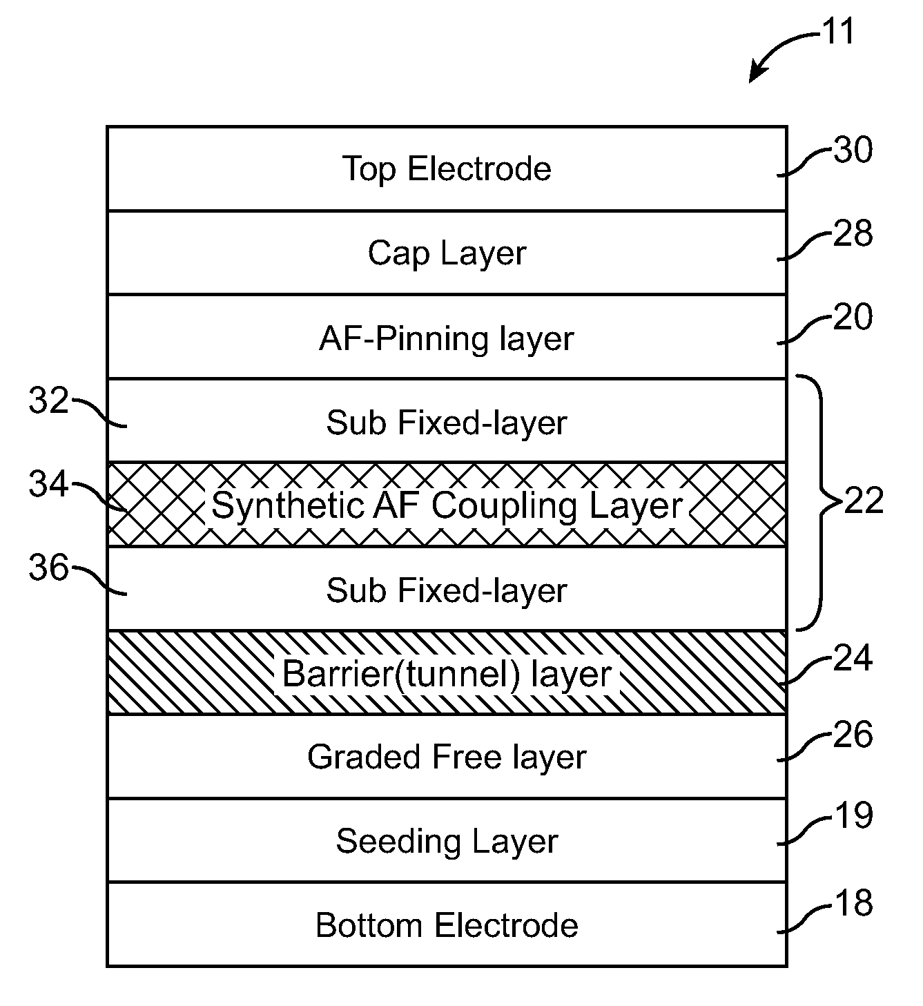
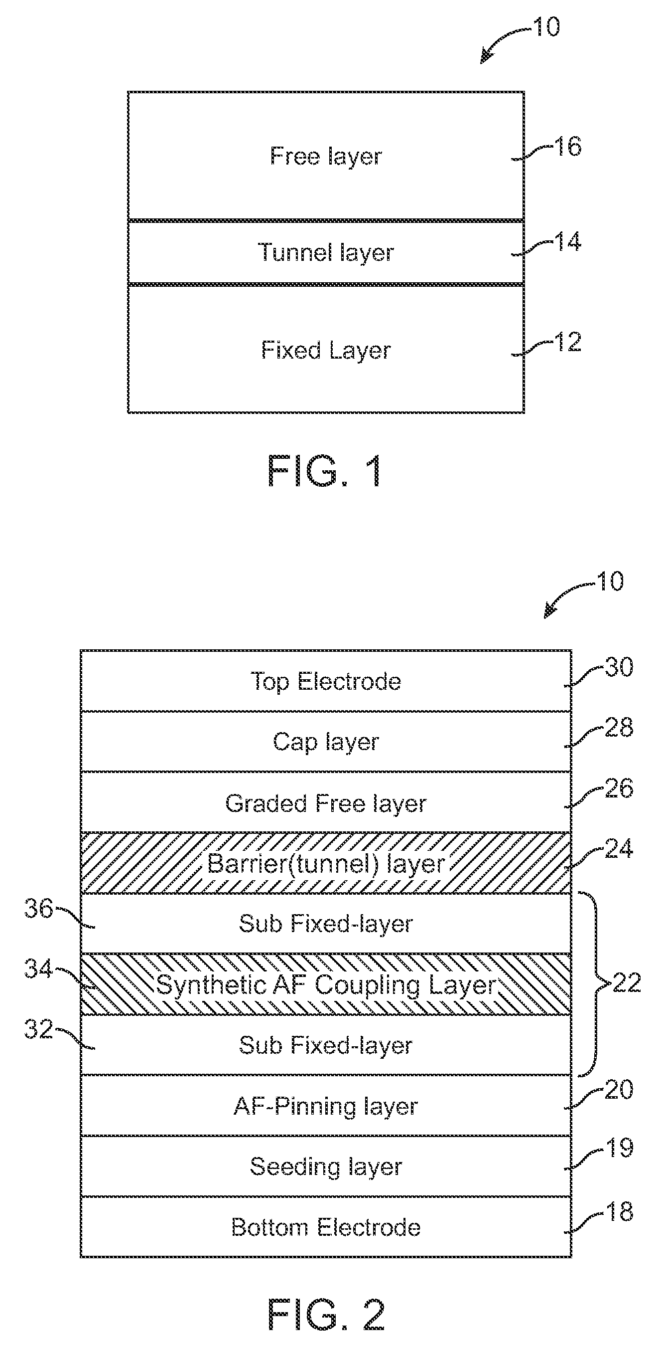
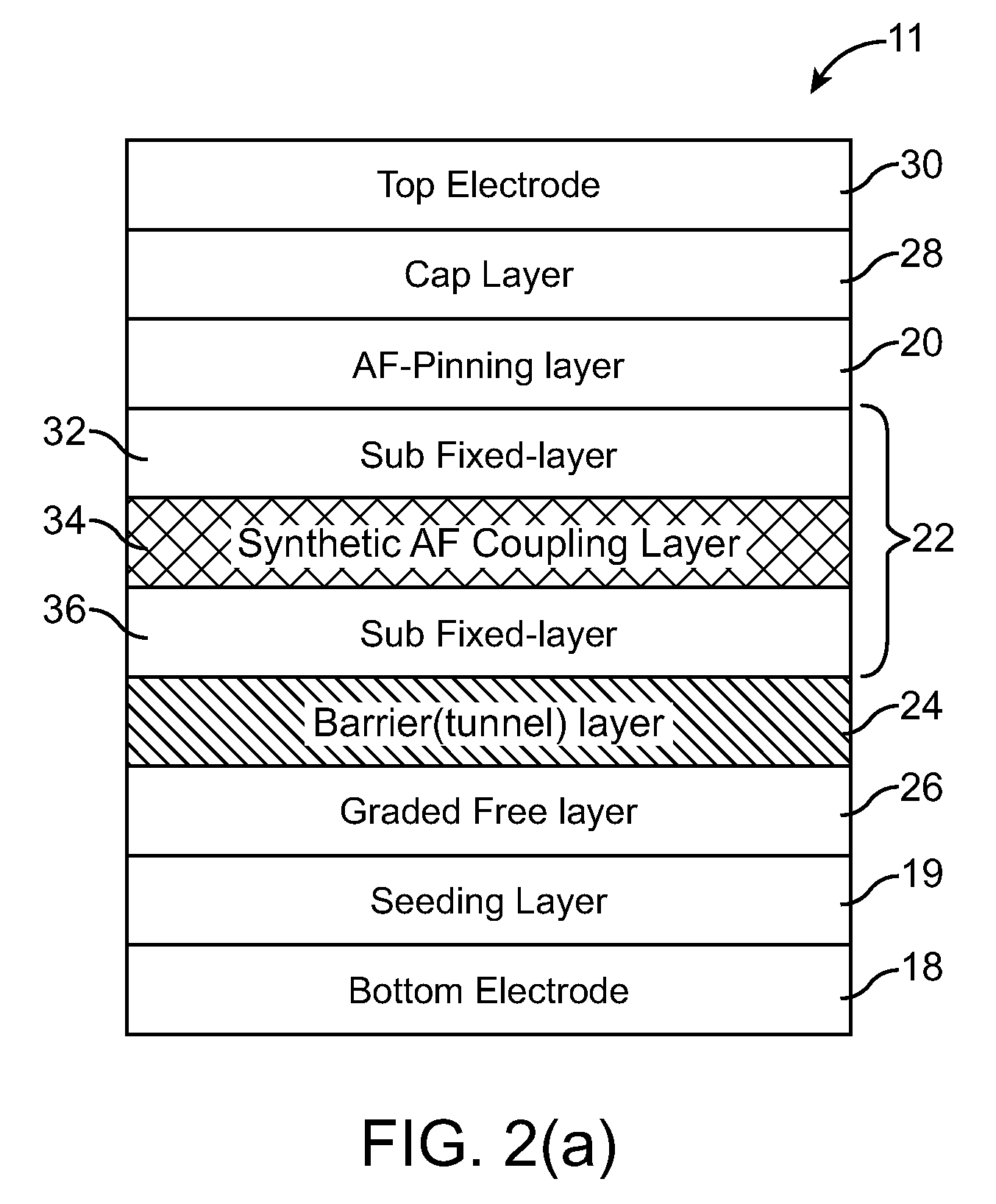
[0033]In the following description of the embodiments, reference is made to the accompanying drawings that form a part hereof, and in which is shown by way of illustration of the specific embodiments in which the invention may be practiced. It is to be understood that other embodiments may be utilized because structural changes may be made without departing from the scope of the present invention. It should be noted that the figures discussed herein are not drawn to scale and thicknesses of lines are not indicative of actual sizes.

[0034]In an embodiment of the present invention, a non-volatile magnetic memory element is disclosed. In one embodiment of the present invention, the memory element includes a graded fixed layer, a tunnel layer and a graded free layer, the fixed layer, tunneling layer and free layer comprising a magnetic tunnel junction (MTJ). The memory element is stackable into arrays of memory elements.

[0035]Referring now to FIG. 1, relevant layers of a non-volatile mag...


PUM


Abstract

One embodiment of the present invention includes a non-volatile magnetic memory element including layers any of which are graded.

Description

CROSS REFERENCE TO RELATED APPLICATIONS[0001]This application is a continuation-in-part of U.S. patent application Ser. No. 11 / 740,861, entitled “A High Capacity Low Cost Multi-Stacked Cross Line Magnetic Memory”, filed on Apr. 26, 2007, which is a continuation-in-part of U.S. patent application Ser. No. 11 / 739,648 entitled “Non-Volatile Magnetic Memory With Low Switching Current And High Thermal Stability”, filed on Apr. 24, 2007, which is a continuation-in-part of U.S. patent application Ser. No. 11 / 678,515 entitled “A High Capacity Low Cost Multi-State Magnetic Memory”, filed on Feb. 23, 2007, which is a continuation-in-part of U.S. patent application Ser. No. 11 / 674,124 entitled “Non-uniform Switching Based Non-Volatile Magnetic Base Memory”, filed on Feb. 12, 2007, the disclosures of which are incorporated herein by reference, as though set forth in full.BACKGROUND OF THE INVENTION[0002]1. Field of the Invention[0003]The present invention relates generally to non-volatile magne...

Claims


Application Information

Patent Timeline
Patent Type & Authority Applications(United States)
IPC IPC(8): H01L29/82H01L21/00
CPCB82Y25/00B82Y40/00H01F10/3236H01F10/3254G11C11/161H01F41/303H01L27/228H01L43/08H01F10/3272H10B61/22H10N50/10H01F10/3277
Inventor RANJAN, RAJIV YADAVKESHTBOD, PARVIZMALMHALL, ROGER KLAS
Owner AVALANCHE TECH
Why Eureka
Try Eureka