Hybrid non-volatile memory device

a non-volatile memory and hybrid technology, applied in the direction of memory architecture accessing/allocation, memory adressing/allocation/relocation, instruments, etc., can solve the problems of increasing design complexity, time to market, and increasing cost, so as to reduce the switching current in the magnetic memory and high memory capacity

Active Publication Date: 2015-07-14
AVALANCHE TECH
View PDF5 Cites 16 Cited by
  • Summary
  • Abstract
  • Description
  • Claims
  • Application Information

AI Technical Summary

Benefits of technology

[0017]To overcome the limitations in the prior art described above, and to overcome other limitations that will become apparent upon reading and understanding the present specification, the present invention discloses a method and a corresponding structure for a magnetic storage memory device that is based on current-induced-magnetization-switching having reduced switching current in the magnetic memory and high memory capacity.

Problems solved by technology

It is believed that NAND flash would be extremely difficult to scale below 45 nanometers (nm).
Likewise, DRAM has issues related to scaling of the trench capacitors leading to very complex designs which are becoming increasingly difficult to manufacture, leading to higher cost.
Design of different memory technology in a product adds to design complexity, time to market and increased costs.
For example, in hand-held multi-media applications incorporating various memory technologies, such as NAND Flash, DRAM and EEPROM / NOR flash memory, complexity of design is increased as are manufacturing costs and time to market.
Another disadvantage is the increase in size of a device that incorporates all of these types of memories therein.
This is primarily due to a dramatic drop in the price of the flash memory.
NOR flash memories are primarily used for applications where non-volatility is essential, but the size of the memory is small and the memory is seldom read or written.
This is mostly used in NAND flash to enhance the memory density, but normally adversely affects the speed of the memory.
Another form of dominant memory is the dynamic RAM (DRAM), which is volatile and costly but has faster random read / write time than non-volatile memory in the form of flash.
Static RAM is the most expensive memory used.
In the current marketplace, NOR tends to be approximately five times more costly than MLC NAND, due primarily to its cell size.
DRAM has a cell size of 8 F2 but is harder to manufacture due to its various trench-capacitor design requirements.
Additionally, as the process geometry decreases, the design of NAND and DRAM memory become more difficult to scale.
For example, NAND has various issues related to capacitive coupling, fewer electrons / bit, poor error-rate performance and worse reliability due to its poor read-write endurance.
It is believed that NAND, especially MLC NAND would be extremely difficult to scale below 45 nano meters (nm).
Likewise, DRAM has issues related to scaling of its trench capacitors leading to very complex designs which are becoming very difficult to manufacture, thereby leading to increased manufacturing costs.
This is a dominant part of the overall cost for mobile multi-media products.
The problem with all of the currently available hybrid designs is the large size and therefore high costs and high power consumption associated therewith.
That is, ROM and RAM are manufactured on multiple chips, and perhaps a monolithic die, resulting in larger real estate being consumed by use of such memory, and therefore increased costs.
This capacity usage on a printed circuit board (PCB) that additionally has other chips (or semiconductor), such as a controller, make such designs approximately 5 to 10 times more expensive than the NAND memory.
Additionally, power consumption is high due to the operations of non-volatile and volatile memory, of which the volatile memory has to stay on the standby power all the time.

Method used


Image

  • Hybrid non-volatile memory device
  • Hybrid non-volatile memory device
  • Hybrid non-volatile memory device

Examples


Embodiment Construction

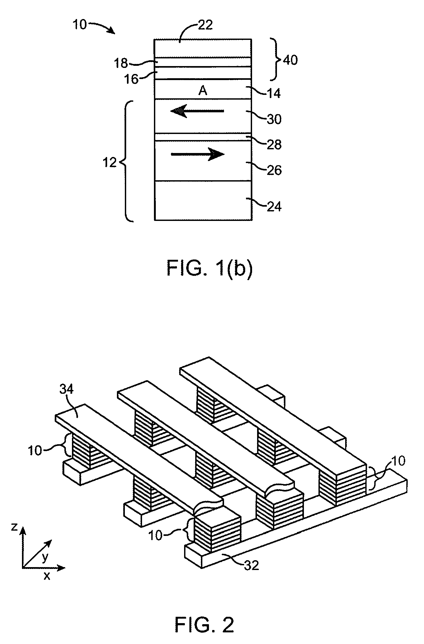
[0050]In the following description of the embodiments, reference is made to the accompanying drawings that form a part hereof, and in which is shown by way of illustration of the specific embodiments in which the invention may be practiced. It is to be understood that other embodiments may be utilized because structural changes may be made without departing from the scope of the present invention. It should be noted that the figures discussed herein are not drawn to scale and thicknesses of lines are not indicative of actual sizes.

[0051]In an embodiment of the present invention, a diode-addressable current-induced magnetization switching (CIMS) memory element is disclosed. In one embodiment of the present invention, the memory element includes a magnetic tunnel junction (MTJ) on top of which is formed a diode for storing digital information. The memory element is stackable into arrays with memory elements in each stack, and each stack separated by deposited dielectric and CMPed (che...


PUM


Abstract

A hybrid non-volatile memory device includes a non-volatile random access memory (NVRAM) having an array of magnetic memory elements, the NVRAM being bit-accessible. The hybrid non-volatile device further includes a non-volatile page-mode memory (PMM) made of resistive memory and organized into pages, the non-volatile PMM being page-accessible. Further included in the hybrid non-volatile memory device is a direct memory access (DMA) engine that is coupled to the NVRAM and the non-volatile PMM and transfers data between the NVRAM and the non-volatile PMM during a DMA operation.

Description

CROSS REFERENCE TO RELATED APPLICATIONS[0001]This application is a continuation-in-part of U.S. patent application Ser. No. 13 / 892,077, filed on May 10, 2013, by Rajiv Yadav Ranjan, and entitled “LOW-COST NON-VOLATILE FLASH-RAM MEMORY”, which is a continuation of U.S. patent application Ser. No. 12 / 182,996, filed on Jul. 30, 2008, and entitled “LOW-COST NON-VOLATILE FLASH-RAM MEMORY”, which is a continuation-in-part of U.S. patent application Ser. No. 11 / 740,861, filed on Apr. 26, 2007 and entitled “A High Capacity Low Cost Multi-Stacked Cross-Line Magnetic Memory,” which claims priority to U.S. Provisional Application No. 60 / 795,755, filed on Apr. 26, 2006 and entitled “High capacity low cost multi-stacked cross-line magnetic memory,” and is a continuation-in-part of U.S. patent application Ser. No. 11 / 674,124 entitled “Non-uniform Switching Based Non-Volatile Magnetic Base Memory,” filed on Feb. 12, 2007 and a continuation-in-part of U.S. patent application Ser. No. 11 / 678,515 ent...

Claims


Application Information

Patent Timeline
Patent Type & Authority Patents(United States)
IPC IPC(8): G11C11/22G11C11/00G06F12/00G11C11/14G06F12/02G11C11/15G11C11/16G11C14/00H01L27/22G11C13/00G11C13/02
CPCG06F12/0246G11C11/005G11C11/15G11C11/16G11C13/0002G11C13/0004G11C14/00H01L27/224G11C11/22G11C13/025G11C2213/71G06F2212/7208G11C11/1659G11C11/161G11C11/1673G11C11/1675G11C11/1653Y02D10/00H10B61/10
Inventor TADEPALLI, RAVISHANKARRANJAN, RAJIV YADAVASNAASHARI, MEHDIVAN LE, NGONKESHTBOD, PARVIZ
Owner AVALANCHE TECH
Why Eureka
Try Eureka