By-product removal for wafer bonding process

a wafer bonding and by-product technology, applied in the field of three-dimensional integrated circuits, structure and manufacturing processes for forming three-dimensional integrated circuits, can solve the problems of reducing the density of two-dimensional components, requiring a minimum size of these components, and reducing the quality of bonding, so as to achieve the effect of improving the bonding quality

Inactive Publication Date: 2008-08-14
TAIWAN SEMICON MFG CO LTD
View PDF5 Cites 32 Cited by
  • Summary
  • Abstract
  • Description
  • Claims
  • Application Information

AI Technical Summary

Benefits of technology

[0013]By forming openings at the interfaces between bonded wafers, the by-products generated by the bonding process are released. Fewer voids are formed at the interfaces, and the bonding quality is improved.

Problems solved by technology

Although dramatic improvement in lithography has resulted in considerable improvement in 2D integrated circuit formation, there are physical limits to the density that can be achieved in two dimensions.
One of these limits is the minimum size needed to make these components.
Also, when more devices are put into one chip, more complex designs are required.
An additional limit comes from the significant increase in the number and length of interconnections between devices as the number of devices increases.
When the number and length of interconnections increase, both circuit RC delay and power consumption increase.
The conventional direct oxide bonding suffers drawbacks.
One problem with such a solution is that if a high temperature process is performed subsequently, H2 or H2O gas may still be released.
As such, the existing technologies are not suitable for 3D integrated circuits, and thus a novel method is needed.

Method used


Image

  • By-product removal for wafer bonding process
  • By-product removal for wafer bonding process
  • By-product removal for wafer bonding process

Examples


Embodiment Construction

[0017]The making and using of the presently preferred embodiments are discussed in detail below. It should be appreciated, however, that the present invention provides many applicable inventive concepts that can be embodied in a wide variety of specific contexts. The specific embodiments discussed are merely illustrative of specific ways to make and use the invention, and do not limit the scope of the invention.

[0018]A novel method for forming three-dimensional (3D) integrated circuits is provided. The intermediate stages of manufacturing a preferred embodiment of the present invention are illustrated. Throughout the various views and illustrative embodiments of the present invention, like reference numbers are used to designate like elements.

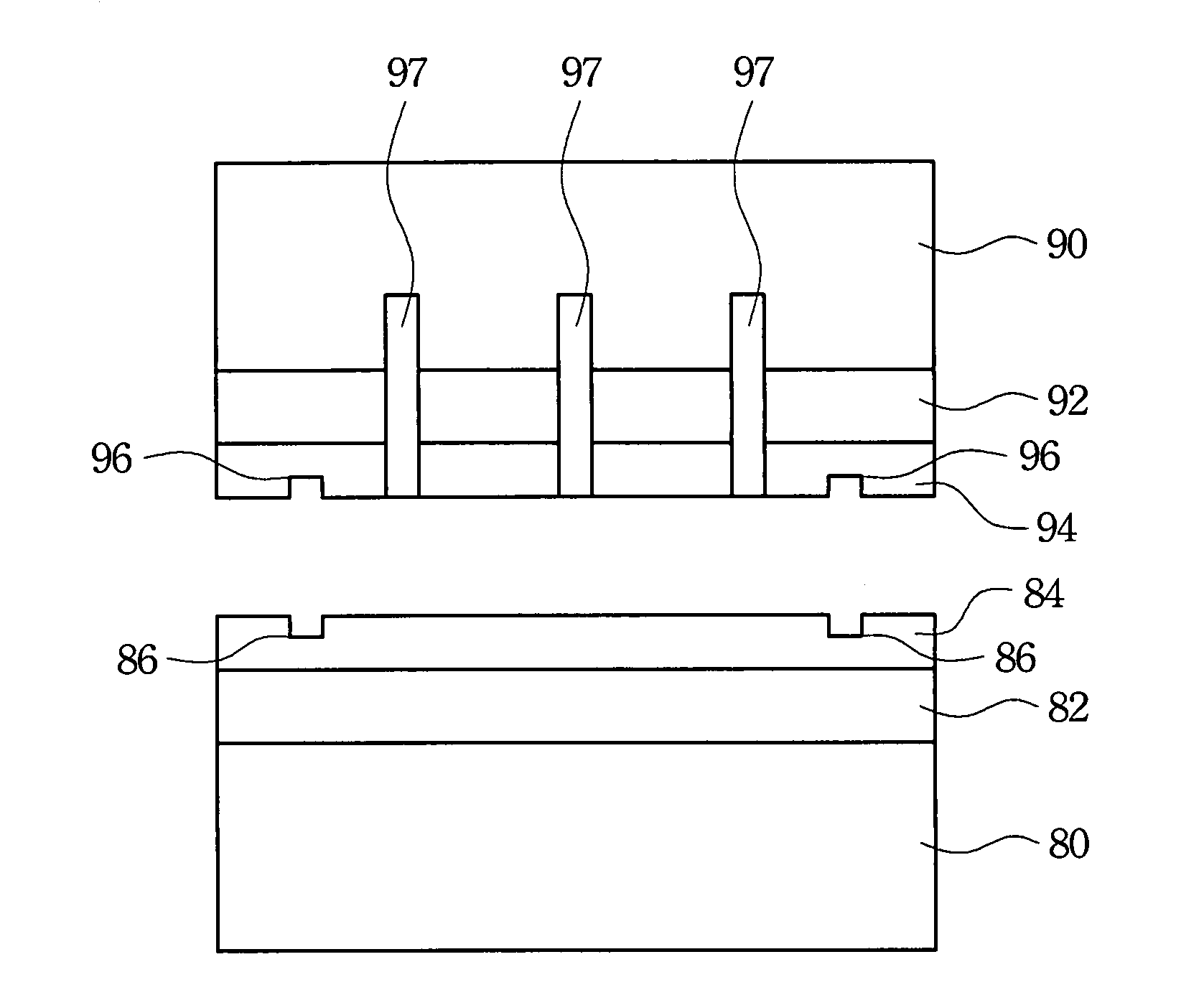
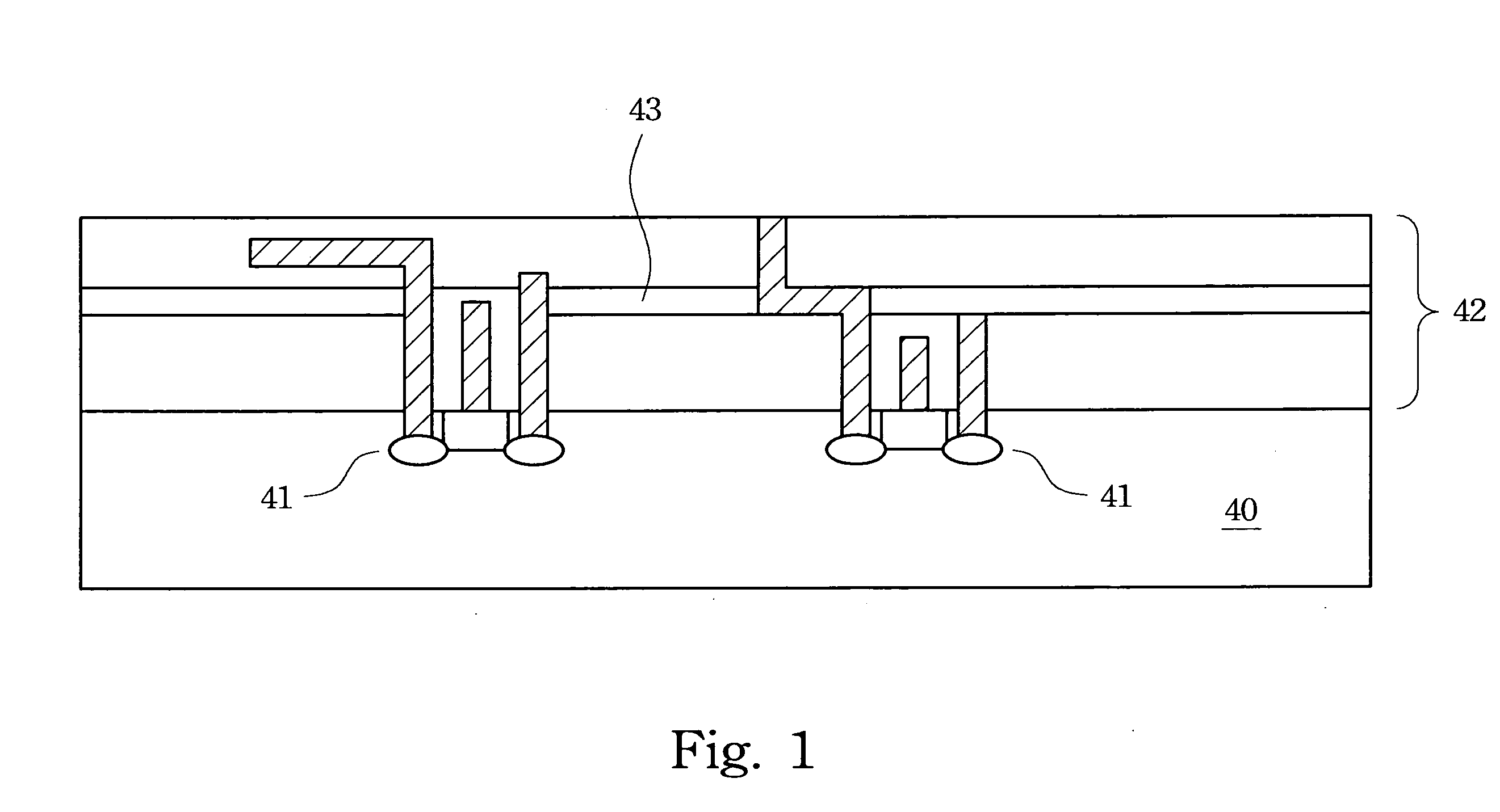
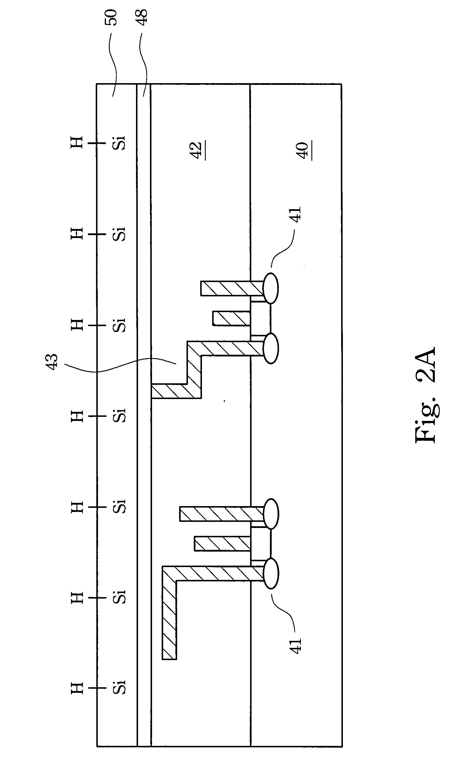
[0019]In FIG. 1, a first wafer is provided. In the preferred embodiment, the first wafer has a semiconductor substrate 40 on which devices 41 are formed. As schematically shown, an interconnect structure 42 is formed over semiconductor substrat...


PUM


Abstract

A three-dimensional (3D) integrated circuit structure includes a first wafer and a second wafer, each comprising a substrate having devices formed thereon and an interconnect structure over the substrate; a composite layer comprising a first dielectric layer bonded to a second dielectric layer, wherein the composite layer is bonded to the first and the second wafers; a first plurality of openings extending from an interface of the first and the second dielectric layers into the first dielectric layer, wherein each opening of the first plurality of openings is in scribe lines of the first wafer; and vias connecting devices in the first and the second wafers.

Description

TECHNICAL FIELD[0001]This invention relates generally to integrated circuits, and more particularly to three-dimensional integrated circuits, and even more particularly to a structure and manufacturing processes for forming three-dimensional integrated circuits.BACKGROUND[0002]Since the invention of the integrated circuit, the semiconductor industry has experienced continuous rapid growth due to constant improvements in the integration density of various electronic components (i.e., transistors, diodes, resistors, capacitors, etc.). For the most part, this improvement in integration density has come from repeated reductions in minimum feature-size, which allow more components to be integrated into a given area.[0003]These integration improvements are essentially two-dimensional (2D) in nature, in that the volume occupied by the integrated components is essentially on the surface of the semiconductor wafer. Although dramatic improvement in lithography has resulted in considerable imp...

Claims


Application Information

Patent Timeline
Patent Type & Authority Applications(United States)
IPC IPC(8): H01L29/00H01L21/762
CPCH01L21/2007H01L27/0688H01L21/8221
Inventor WU, WENG-JINCHIOU, WEN-CHIHYU, CHEN-HUA
Owner TAIWAN SEMICON MFG CO LTD
Why Eureka
Try Eureka