Method For Manufacturing Thin Keypad Assembly And Such Assembly

a technology of keypad and assembly, which is applied in the field of keypad assembly, can solve the problems of poor contact between the circuit board and the corrosion damage of the components, affecting the smoothness of pressing the keys, and affecting the smoothness of the keys, so as to achieve the effect of keeping the surface of the keypad clean

Inactive Publication Date: 2008-08-14
ICHIA TECH
View PDF13 Cites 24 Cited by
  • Summary
  • Abstract
  • Description
  • Claims
  • Application Information

AI Technical Summary

Benefits of technology

[0007]The present invention is to provide a thin keypad assembly with no seams and contamination between the keys, by which the

Problems solved by technology

Although the seam B will not affect the operation of neighboring keys, foreign matters (such as dust or fine particles) are easily filled into the seam, affecting the smoothness in pressing the keys.
Alternatively, water may penetrate into the electronic product th

Method used


Image

  • Method For Manufacturing Thin Keypad Assembly And Such Assembly
  • Method For Manufacturing Thin Keypad Assembly And Such Assembly
  • Method For Manufacturing Thin Keypad Assembly And Such Assembly

Examples


Embodiment Construction

[0031]The technical contents and detailed description of the present invention will be explained with reference to the accompanying drawings.

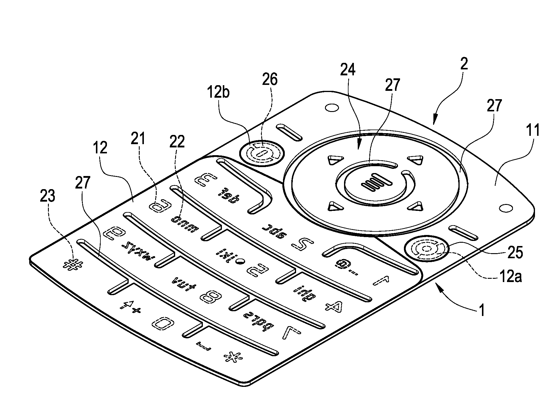
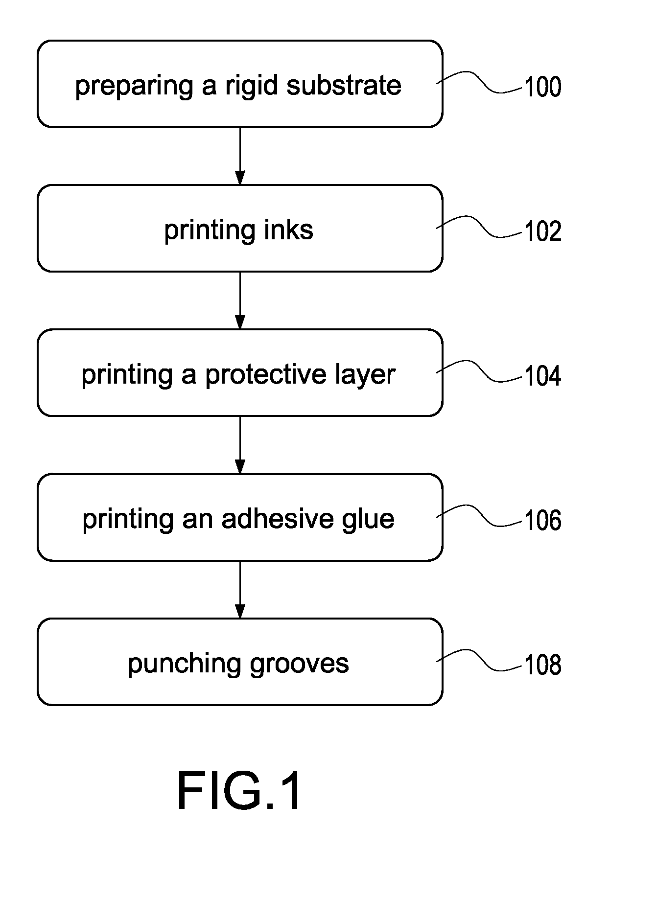
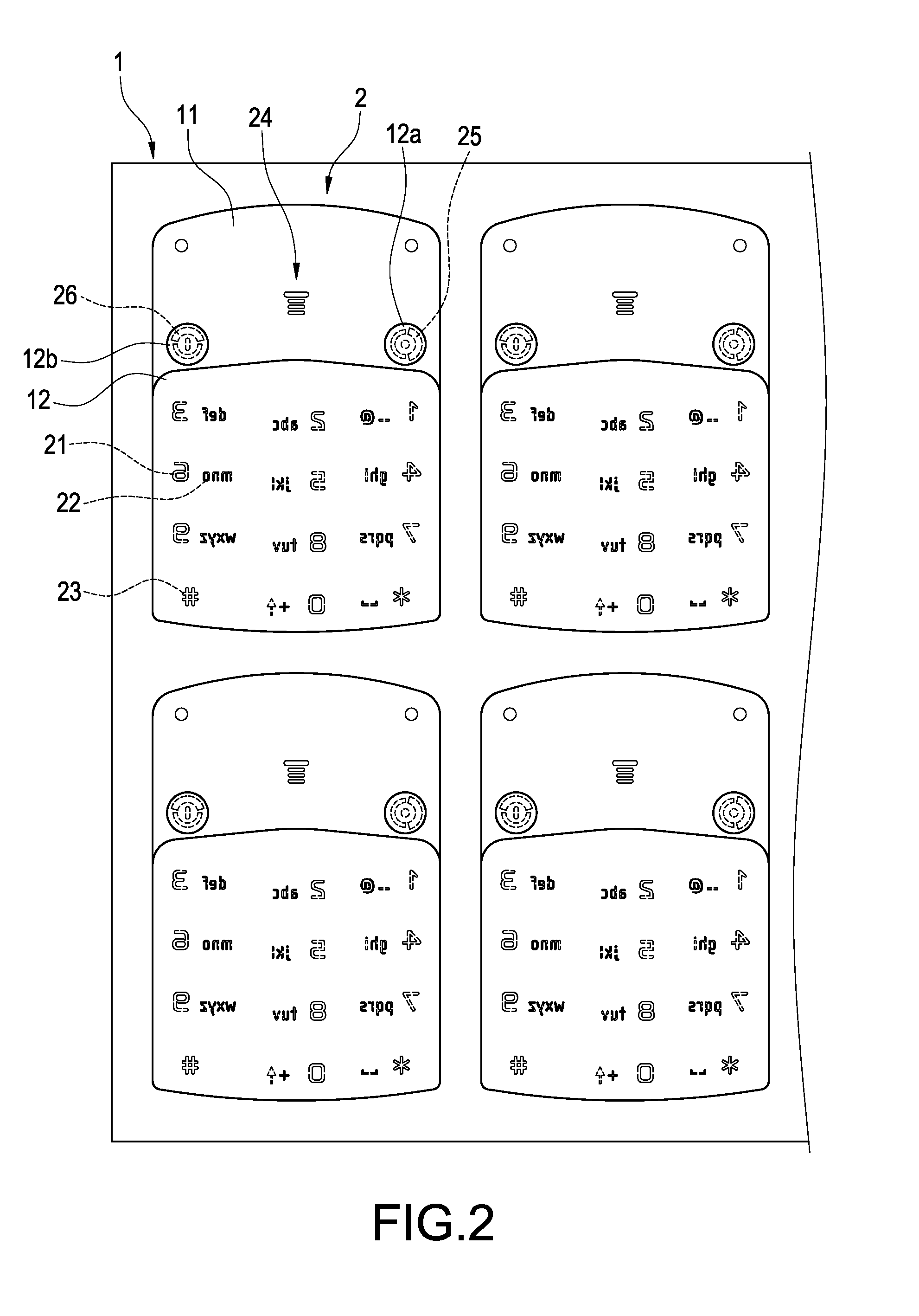
[0032]FIG. 1 is a schematic view showing the manufacturing process of the keypad panel of the present invention, and FIG. 2 is a front view of the keypad panel of the present invention. It can be seen that these drawings disclose a method for manufacturing a thin keypad panel. First, in the step 100, a transparent hard substrate 1 is prepared. The hard substrate 1 is a PC film plastic material.

[0033]In the step 102, a first layer 11 of black ink is printed on the surface of the hard substrate to form a plurality of panels 2, while the panels 2 are made to have hollowed numerals 21 (“0”, “1”, “2” . . . “9”), English letters 22, various symbols 23, a navigation-key pattern 24, a dialing pattern 25 and an ending pattern 26. The numerals 21, English letters 22 and various symbols 23 on the first layer 11 are printed thereon with a second layer 12 o...


PUM


Abstract

A method for manufacturing a thin keypad with no seams on a panel surface and such assembly includes the following steps. Inks of different colors are printed onto the surface of a rigid substrate so as to shape panel forms and light-transmitting numerals, letters, symbols, a navigation-key pattern, a dialing pattern and an ending pattern. The panel surface is formed with a plurality of grooves after machining and cutting. Then, inks of different colors are printed onto the surface of a soft substrate so as to form a lining sheet of a light-shielding layer and a reflective layer corresponding to patterns of the panel. The thus-formed panel and lining sheet are disposed into a mold. Rubber is filled in the mold and, after pressing, bound with the bottom of the lining sheet to form a light-guiding layer. At the same time, the light-shielding layer, the reflective layer and the rubber are extruded on the panel surface, so that no seams exist between the keys of the panel surface. Finally, laser is radiated to dot on the light-guiding layer to form thereon light-guiding micro structures having a light-condensing effect.

Description

BACKGROUND OF THE INVENTION[0001]1. Field of the Invention[0002]The present invention relates to a keypad assembly, and in particular to a method for manufacturing a thin keypad assembly.[0003]2. Description of Prior Art[0004]With the continuous progress of communication technology, many electronic products tend to be made compact, thereby to reduce the size and weight thereof and facilitate a user to carry. In order to reduce the size and weight of the electronic product, the volume of the internal integrated circuit has to be reduced. In addition, the area and thickness of the keypad acting as an operational interface of the electronic product should be also reduced, so that it can be easily mounted in a communication device.[0005]U.S. Pat. No. 7,070,349 B2, entitled “THIN KEYPAD AND COMPONENTS FOR ELECTRONICS DEVICES AND METHODS” and shown in FIG. 16, discloses a conventional keypad assembly, in which after the keypad is assembled, a seam B exists between the key layer A and key ...

Claims


Application Information

Patent Timeline
IPC IPC(8): H01H13/70
CPCH01H13/7006H01H2231/026H01H2209/068H01H2219/028H01H2219/03H01H2219/034H01H2219/056H01H2219/062H01H2221/002H01H2221/004H01H2223/002H01H2229/00H01H2229/048H01H2231/022H01H13/88
Inventor TSAO, KAI-JIE
Owner ICHIA TECH
Why Eureka
Try Eureka