Display device and driving method thereof

a technology of display device and driving method, which is applied in the direction of static indicating device, electroluminescent light source, instruments, etc., can solve the problems of complex configuration of pixel circuit, hinder the achievement of higher definition of display device, and consequently difficult to apply the 5tr driving configuration to display device used in small electronic devices such as portable devices

Inactive Publication Date: 2008-08-21
SONY CORP
View PDF10 Cites 173 Cited by
  • Summary
  • Abstract
  • Description
  • Claims
  • Application Information

AI Technical Summary

Benefits of technology

[0019]In addition, it is particularly desirable to provide a mechanism that can ease effects of an operation of driving a pixel circuit on image quality (suppress luminance variations in particular) while simplifying the pixel circuit.
[0020]Further, it is desirable to provide a mechanism that can suppress changes in luminance due to variations in the characteristics of a drive transistor and a light emitting element in simplifying the pixel circuit.
[0034]In addition, the control unit preferably controls the bootstrap operation so as to achieve an operation of correcting secular changes of the electrooptic element in an emission period. Thus, it is desirable that the control unit continuously hold the sampling transistor in the non-conducting state during the period during which the driving current based on the information retained in the storage capacitor flows through the electrooptic element, whereby the voltage between the control input terminal and the output terminal can be held constant and thus the operation of correcting the secular changes of the electrooptic element is achieved.
[0036]According to an embodiment of the present invention, when the threshold value correcting operation is repeated a plurality of times on a time division basis, during the period of the plurality of threshold value correcting operations, the light emission controlling transistor and the sampling transistor are held in the conducting state in periods of the fixed potential for threshold value correction, while the light emission controlling transistor and the sampling transistor are held in the non-conducting state in periods in which the video signal is at the signal potential, in such a manner that the light emission controlling transistor and the sampling transistor are interlocked with each other. It is thus possible to avoid a situation such for example as a failure of threshold value correction as a result of bootstrap operation performed during intervals between a plurality of threshold value correcting periods.

Problems solved by technology

Therefore the configuration of the pixel circuit is complex.
Many constituent elements of the pixel circuit hinders the achievement of higher definition of the display device.
It is consequently difficult to apply the 5TR driving configuration to display devices used in small electronic devices such as portable devices (mobile devices) and the like.

Method used


Image

  • Display device and driving method thereof
  • Display device and driving method thereof
  • Display device and driving method thereof

Examples


Embodiment Construction

[0044]Preferred embodiments of the present invention will hereinafter be described in detail with reference to the drawings.

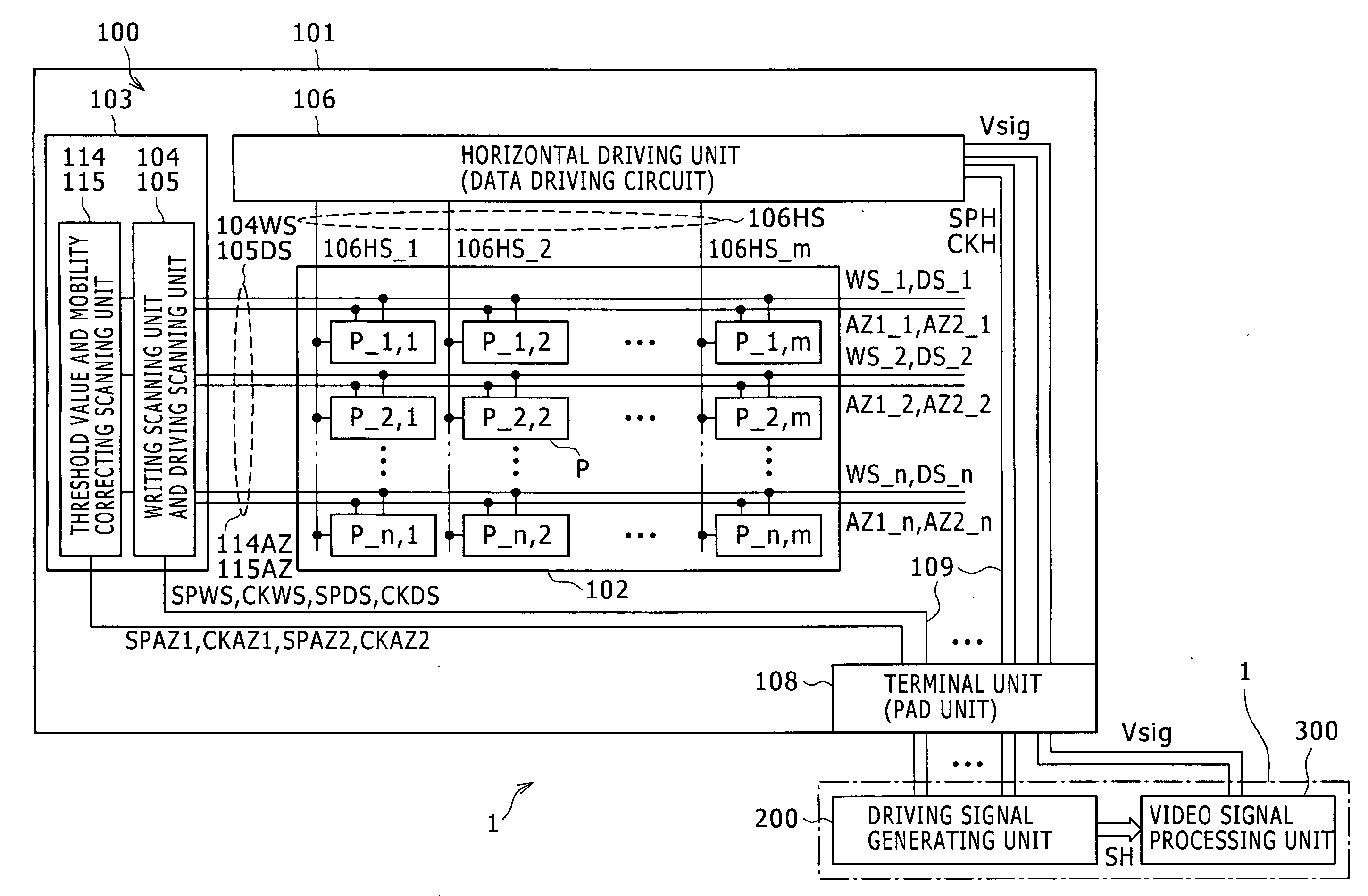
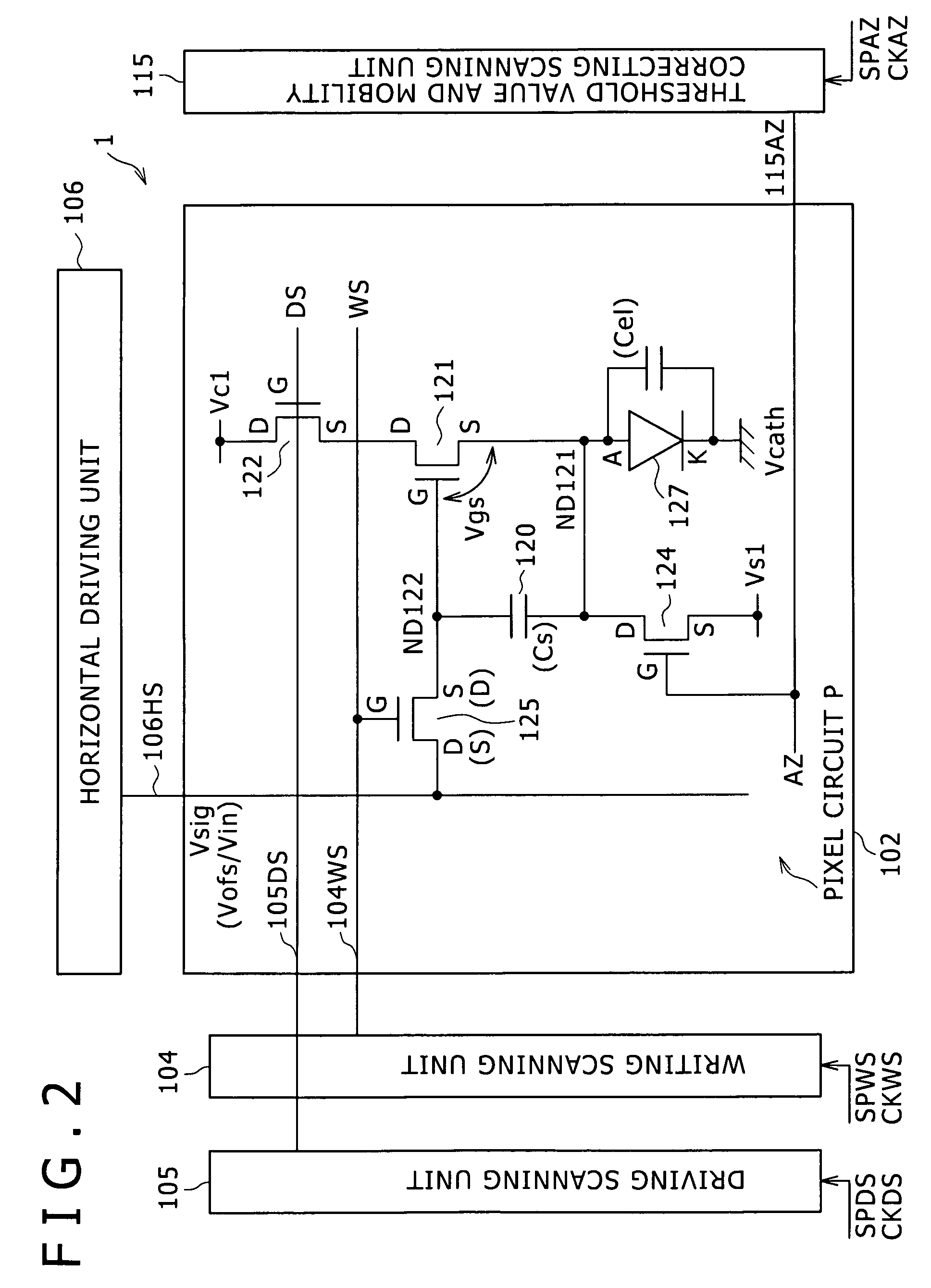
[0045]FIG. 1 is a block diagram schematically showing a configuration of an active matrix type display device as an embodiment of a display device according to the present invention. In the present embodiment, description will be made by taking as an example a case where the present invention is applied to an active matrix type organic EL display (hereinafter referred to as an organic EL display device) that for example uses an organic EL element as a display element of a pixel and a polysilicon thin film transistor (TFT) as an active element and which display is constituted with the organic EL element formed on a semiconductor substrate where the thin film transistor is formed.

[0046]Incidentally, while concrete description will be made in the following by taking the organic EL element as the display element of the pixel as an example, the organic EL element is...


PUM


Abstract

Disclosed herein is a display device including: a pixel array unit having pixel circuits arranged in a form of a matrix; and a control unit having a writing scanning unit for outputting, to the sampling transistor, a writing scanning pulse. The control unit effects control to supply a control input terminal of the drive transistor with a fixed potential for a threshold value correcting operation for retaining a voltage corresponding to a threshold voltage of the drive transistor in the storage capacitor. When setting a voltage across the storage capacitor to the threshold voltage of the drive transistor by repeating the threshold value correcting operation a plurality of times on a time division basis, the control unit effects control to perform each the threshold value correcting operation and the sampling transistor to a conducting state.

Description

CROSS REFERENCES TO RELATED APPLICATIONS[0001]The present invention contains subject matter related to Japanese Patent Application JP 2007-038863 filed with the Japan Patent Office on Feb. 20, 2007, the entire contents of which being incorporated herein by reference.BACKGROUND OF THE INVENTION[0002]1. Field of the Invention[0003]The present invention relates to a display device having a pixel array unit in which pixel circuits (referred to also as pixels) including an electrooptic element (referred to also as a display element or a light emitting element) are arranged in the form of a matrix, and a driving method of the display device, and particularly to an active matrix type display device that is formed by arranging pixel circuits having an electrooptic element changing in luminance according to the magnitude of a driving signal as a display element in the form of a matrix and which has an active element in each pixel circuit, display driving being performed in a pixel unit by th...

Claims


Application Information

Patent Timeline
Patent Type & Authority Applications(United States)
IPC IPC(8): G09G3/30
CPCG09G3/3233G09G3/325G09G2300/0819G09G2320/043G09G2320/0233G09G2320/0295G09G2310/0262G09G3/30G09G3/20H05B33/12G09G3/32
Inventor TOYOMURA, NAOBUMIUCHINO, KATSUHIDEYAMAMOTO, TETSURO
Owner SONY CORP
Why Eureka
Try Eureka