Semiconductor Memory Device and Method of Fabricating the Same

Inactive Publication Date: 2008-08-28
SK HYNIX INC
View PDF9 Cites 6 Cited by
  • Summary
  • Abstract
  • Description
  • Claims
  • Application Information

AI Technical Summary

Benefits of technology

[0006]In an embodiment of the invention, an isolation layer is formed in a trench of an isolation region. An EFH is controlled so that the height of a central portion of the isolation layer is lowered than edge portions of the isolation layer. Thus, edge portions of a tunnel insulating layer formed in an active region can be prevented from being exposed while lowering the height of the central portion the isolation layer, and further the etch damage to the tunnel insulating layer can be prevented. A shield layer is formed between floating gates. Accordingly, an interference phenomenon between the floating gates can be prevented.
[0010]In an embodiment of the invention, a step may be generated between the first insulating layer and the second insulating layer to lower the height of the first insulating layer and the second insulating layer. The step may cause the height of the second insulating layer to lower than the height of the first insulating layer.

Problems solved by technology

As semiconductor memory devices have become highly integrated, an increased interference is generated, for example, between word lines in NAND flash memory devices.
This fabrication method is vulnerable to, in particular, interference which may be caused by the capacitance existing between cells.
However, there are some limitations when controlling the EFH to a certain depth.
However, the tunnel oxide layer may be exposed and damaged at the time of etching the isolation layer for lowering the EFH.
Once the tunnel oxide layer is damaged, an operating capability of a device is significantly lowered and the device may malfunction.

Method used


Image

  • Semiconductor Memory Device and Method of Fabricating the Same
  • Semiconductor Memory Device and Method of Fabricating the Same
  • Semiconductor Memory Device and Method of Fabricating the Same

Examples


Embodiment Construction

[0019]While the patent is susceptible to various modifications and alternative forms, certain embodiments as shown by way of example in the drawings and these embodiments will be described in detail herein. It will be understood, however, that this disclosure is not intended to limit the patent to the particular forms described, but to the contrary, the patent is intended to cover all modifications, alternatives, and equivalents falling within the spirit and scope of the patent defined by the appended claims.

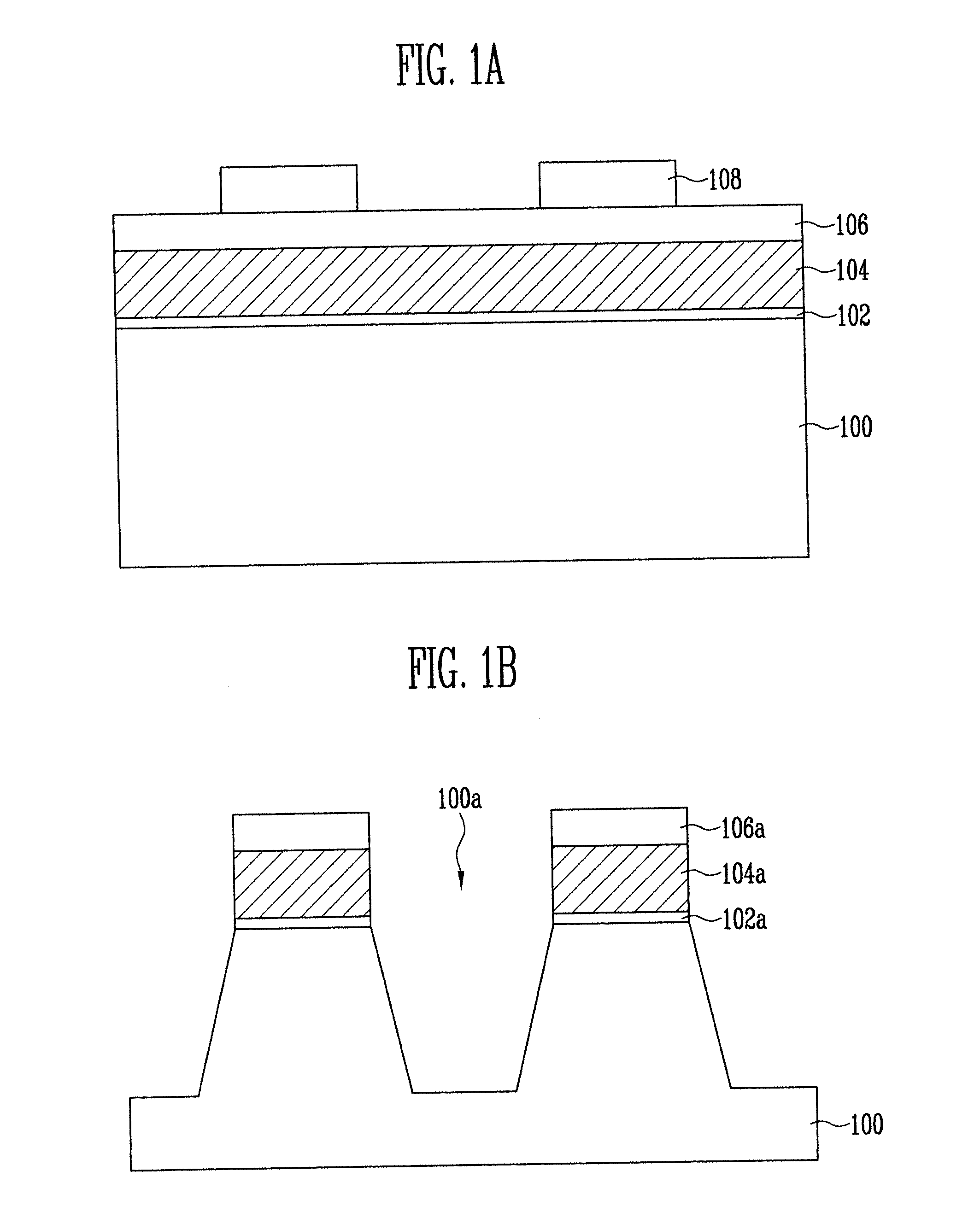
[0020]Referring to FIG. 1A, a tunnel insulating layer 102, a first conductive layer 104 for a floating gate, a first mask film 106, and a second mask film 108 are formed over a semiconductor substrate 100. The tunnel insulating layer 102 may be formed, for example, of an oxide layer and the first mask film 106 may be formed, for example, of a nitride layer. The second mask film 108 serves as a mask for patterning the floating gate 104 and an active region of the semiconductor su...


PUM


Abstract

This patent relates to a semiconductor memory device and a method of fabricating the same. The semiconductor memory device may include a semiconductor substrate in which a tunnel insulating layer, and a first conductive layer. At least a portion of the semiconductor substrate is removed to form a trench. A first insulating layer may be formed on an internal surface of the trench. A shield layer may be made of a conductive material is formed on the first insulating layer. A second insulating layer may be formed on the shield layer and is configured to gap fill the trench.

Description

CROSS-REFERENCES TO RELATED APPLICATIONS[0001]This patent claims priority to Korean patent application number 10-2007-17913, filed on Feb. 22, 2007, the disclosure of which is incorporated by reference in its entirety.TECHNICAL FIELD[0002]This patent relates to a semiconductor memory device and a method of fabricating the same and, more particularly, to a semiconductor memory device wherein a shield layer is formed between cells and a method of fabricating the same.BACKGROUND OF THE INVENTION[0003]As semiconductor memory devices have become highly integrated, an increased interference is generated, for example, between word lines in NAND flash memory devices. This interference is generated more likely in a multi-level cell (MLC) in which a number of bits are stored in one cell than in a single level cell (SLC) in which one bit is stored in one cell.[0004]Generally, a self-aligned method is used when fabricating a flash memory device having a narrow line width. This fabrication metho...

Claims


Application Information

Patent Timeline
IPC IPC(8): H01L29/78H01L21/762
CPCH01L21/76232H01L21/763H01L29/66825H01L27/11521H01L27/115H10B69/00H10B41/30H01L21/762
Inventor HWANG, JOO WON
Owner SK HYNIX INC
Why Eureka
Try Eureka