Eureka AIR delivers breakthrough ideas for toughest innovation challenges, trusted by R&D personnel around the world.

Semiconductor wafer structure with balanced reflectance and absorption characteristics for rapid thermal anneal uniformity

Inactive Publication Date: 2008-08-28
IBM CORP
View PDF23 Cites 2 Cited by
  • Summary
  • Abstract
  • Description
  • Claims
  • Application Information

AI Technical Summary

Benefits of technology

[0008]More particularly, an embodiment of the semiconductor wafer structure of the invention comprises multiple sections each with multiple layers of thin films. Specifically, the wafer structure may comprise at least one first section (e.g., a device region) comprising a first film on a first portion of an insulator layer above a semiconductor substrate and at least one second section (e.g., a shallow trench isolation region) comprising a second different film on a second portion of the same insulator layer. Furthermore, a given source of thermal annealing with a given wavelength as measured in vacuum, will have a first wavelength in the first film, referred to herein as a first reflectivity wavelength, and a second wavelength in the second film, referred to here in as a second reflectivity wavelength. The first film and the substrate can each comprise a semiconductor (e.g., silicon) with a first index of refraction, and a first reflectivity wavelength. Similarly, the second film and the insulator layer can each comprise an insulator (e.g., silicon dioxide) with a second index of refraction, and a second reflectivity wavelength. However, the thicknesses of these films can be selectively varied so that the net reflectivity of the different sections of the wafer will be approximately uniform, thereby, allowing for uniform heating during rapid thermal anneals.
[0009]More specifically, a first thickness of the first film can be selectively different from a second thickness of the second film such that a first net reflectivity of the first sections (i.e., of the first film, the insulator layer and the substrate) is approximately equal to a second net reflectivity of the second sections (i.e., of the second film, the insulator layer and the substrate). That is, the film thicknesses are selected so as to eliminate or minimize reflectivity differences between the different films. This can be accomplished, for example, if the first thickness of the first film comprises a multiple of one-half the first reflectivity wavelength, if the third thickness of the insulator layer comprises a multiple of one-quarter of the second reflectivity wavelength and if a combined thickness of the insulator layer and the second film comprises an odd multiple of one-quarter of the second reflectivity wavelength (i.e., if the second thickness of the second film comprises a multiple of one-half the second reflectivity wavelength).
[0012]Another embodiment of the semiconductor wafer structure of the invention similarly comprises multiple sections each with multiple layers of thin films that have different indices of refraction, and hence typically differing reflectivities. However, instead of varying the thicknesses of the thin films, this embodiment of the structure incorporates a reflectance layer into the structure above the substrate to balance differences (i.e., to eliminate or minimize the differences) in reflectivity from section to section.
[0013]Specifically, the wafer structure can comprise a semiconductor substrate and at least one first section and at least one second section. The first section (e.g., a device region) can comprise a first material (e.g., silicon) with a first index of refraction (and, thus, a first reflectivity) and first thickness above a first portion of the semiconductor substrate. The second section (e.g., a shallow trench isolation region) can comprise a second material (e.g., silicon dioxide) with a second index of refraction (and, thus, a second reflectivity) and second thickness above a second portion of the semiconductor substrate and adjacent to the first material. The reflectivities of the first and second material are different, but the thicknesses are the same. The semiconductor wafer structure further incorporates a reflectance layer between the semiconductor substrate and the first and second materials. This reflectance layer comprises a pre-selected material that balances the reflectivity characteristics (i.e., eliminates or minimizes differences in the reflectivity and absorption characteristics) between the first and second sections.

Problems solved by technology

However, variations in the reflectance and absorption in different regions of a wafer, e.g., due to different materials and / or different thicknesses of materials, can result in non-uniform temperature changes across the wafer.
These non-uniform temperature changes can result in temperature variations on the wafer of 11° C. or more.
Different silicon to silicon dioxide ratios in different regions of the wafer will result in non-uniform temperature changes during an RTA.
These non-uniform temperature changes can cause variations in dopant activation, dopant diffusion, damage repair, etc. across the wafer and can, thereby, cause variations in threshold voltages, sheet resistances, drive currents, leakage currents, etc. between devices on different regions of the wafer.
Thus, non-uniform temperature changes can cause significant, location-dependent, variations in device performance.

Method used


Image

  • Semiconductor wafer structure with balanced reflectance and absorption characteristics for rapid thermal anneal uniformity
  • Semiconductor wafer structure with balanced reflectance and absorption characteristics for rapid thermal anneal uniformity
  • Semiconductor wafer structure with balanced reflectance and absorption characteristics for rapid thermal anneal uniformity

Examples


Embodiment Construction

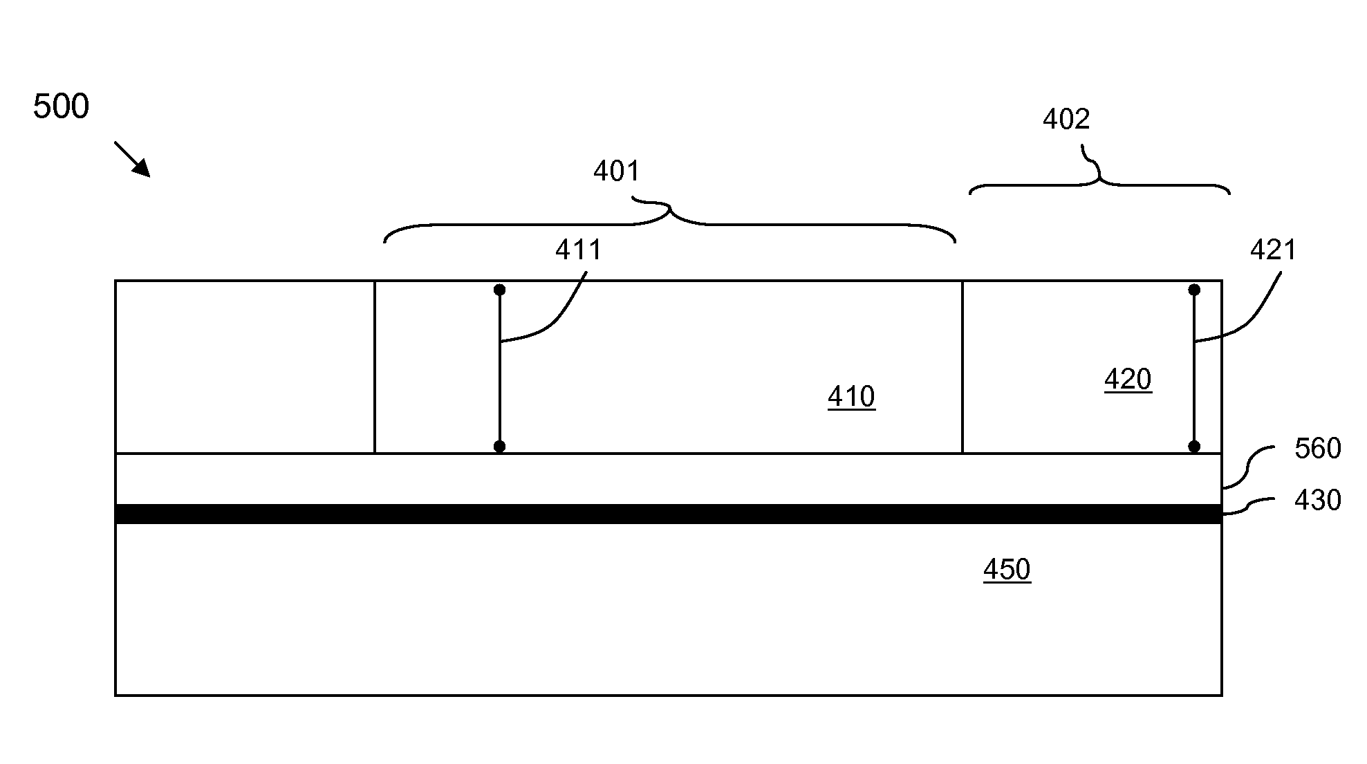
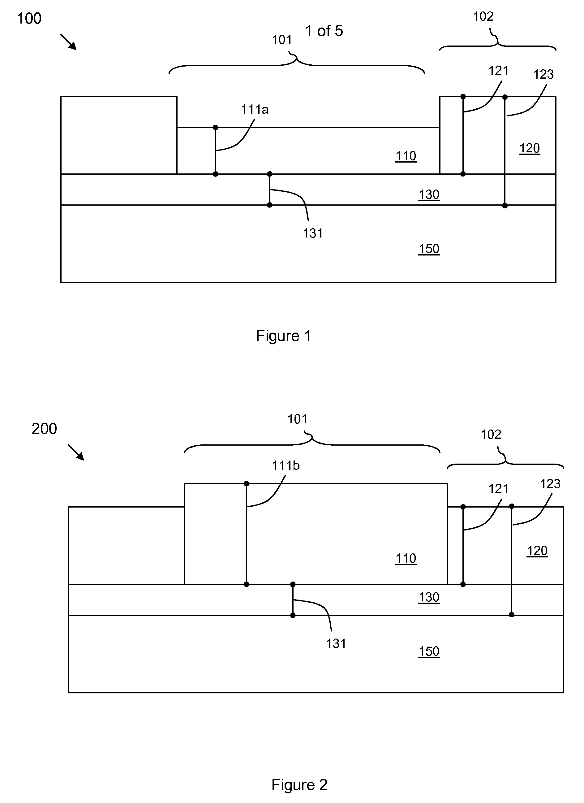
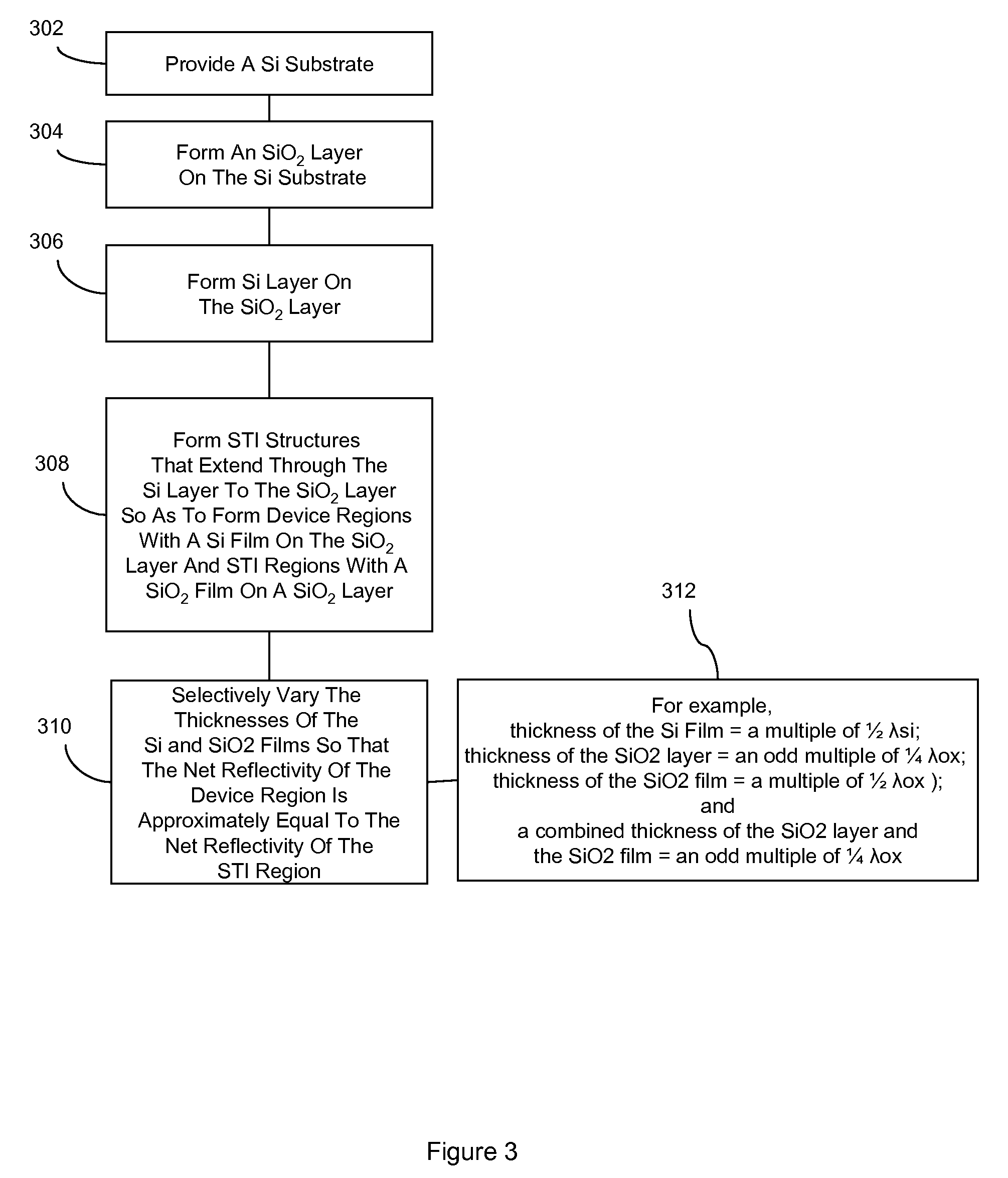
[0029]The embodiments of the invention and the various features and advantageous details thereof are explained more fully with reference to the non-limiting embodiments that are illustrated in the accompanying drawings and detailed in the following description. It should be noted that the features illustrated in the drawings are not necessarily drawn to scale. Descriptions of well-known components and processing techniques are omitted so as to not unnecessarily obscure the embodiments of the invention. The examples used herein are intended merely to facilitate an understanding of ways in which the embodiments of the invention may be practiced and to further enable those of skill in the art to practice the embodiments of the invention. Accordingly, the examples should not be construed as limiting the scope of the embodiments of the invention.

[0030]As mentioned above, variations in reflectance and absorption characteristics can be caused by a variety of different factors including, di...


PUM


Abstract

Disclosed are embodiments of semiconductor wafer structures and associated methods of forming the structures with balanced reflectance and absorption characteristics. The reflectance and absorption characteristics are balanced by manipulating thin film interferences. Specifically, thin film interferences are manipulated by selectively varying the thicknesses of the different films. Alternatively, reflectance and absorption characteristics can be balanced by incorporating an additional reflectance layer into the wafer structure above the substrate.

Description

BACKGROUND[0001]1. Field of the Invention[0002]The embodiments of the invention generally relate to semiconductor wafers and, more particularly, to semiconductor wafer structures and methods of forming the structures that balance variations in reflectance and absorption characteristics.[0003]2. Description of the Related Art[0004]Semiconductor wafer fabrication often involves the use of a rapid thermal anneal (RTA) process to affect the electrical properties of active devices on the wafer. More specifically, an RTA process can be used to activate dopants, diffuse dopants, anneal structures, repair damage from ion implantation processes, etc. RTAs are typically performed by powerful halogen lamp-based heating equipment, flash lamps, or lasers which direct radiation onto a wafer surface in order to change the wafer temperature. However, variations in the reflectance and absorption in different regions of a wafer, e.g., due to different materials and / or different thicknesses of materia...

Claims


Application Information

Patent Timeline
IPC IPC(8): H01L23/58H01L21/31
CPCH01L22/12H01L21/324
Inventor ANDERSON, BRENT A.NOWAK, EDWARD J.
Owner IBM CORP
Why Eureka
Eureka Blog
Learn More