Nonvolatile semiconductor memory device having protection function for each memory block
a nonvolatile semiconductor and memory device technology, applied in the direction of unauthorized memory use protection, digital storage, instruments, etc., can solve the problems of no protection function of flash memory as a replacement for magnetic storage media, no sufficiently effective measures in chip size, operation speed, and convenience for users
- Summary
- Abstract
- Description
- Claims
- Application Information
AI Technical Summary
Benefits of technology
Problems solved by technology
Method used
Image


Examples
Embodiment Construction
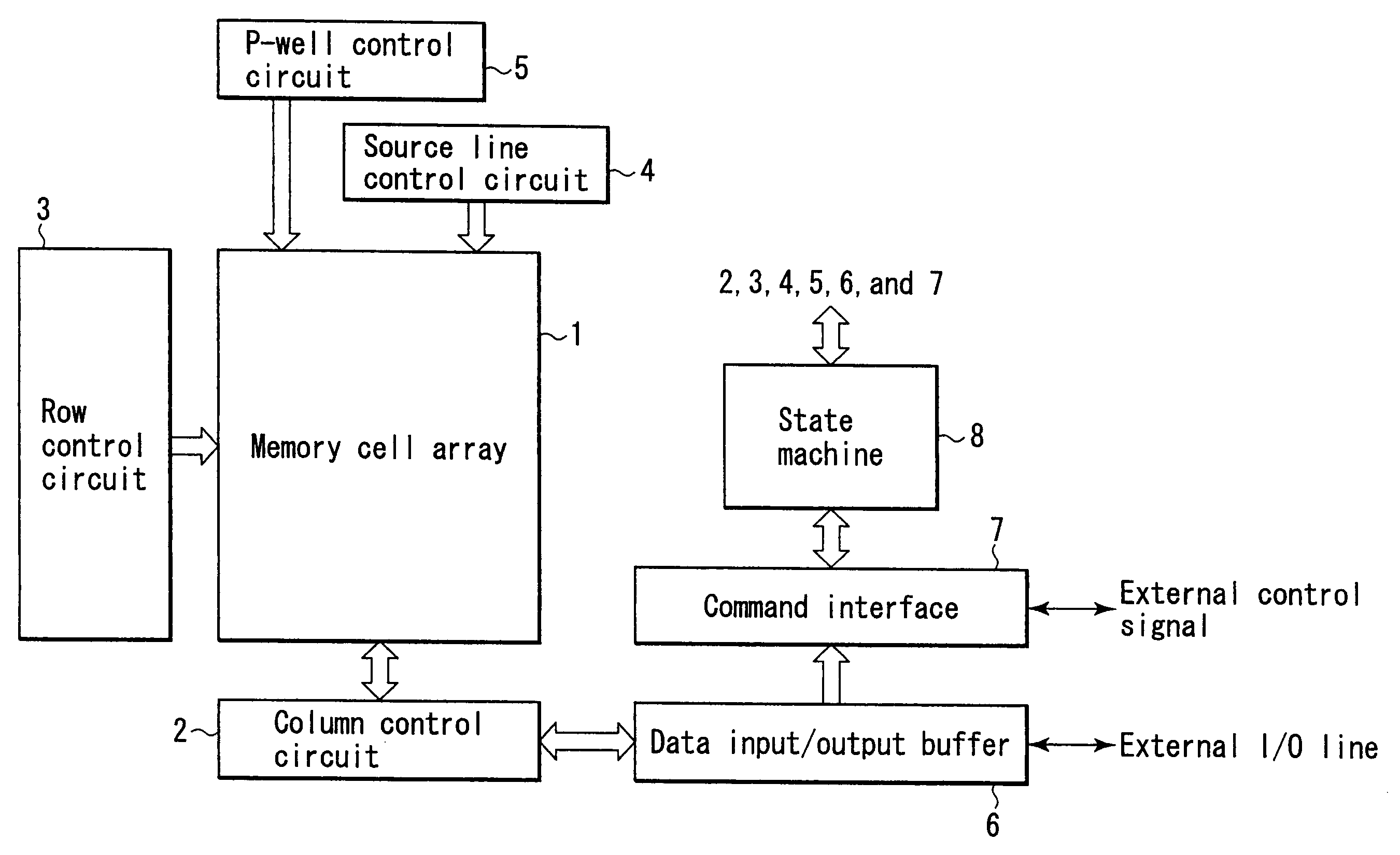
[0036]FIG. 1 is a block diagram showing the structure of a flash memory as a nonvolatile semiconductor memory device according to the embodiment of the present invention. A NAND flash memory is illustrated as an example, and a main part related to the protection function is shown.
[0037]A memory cell array 1 is constructed by arraying flash memory cells in a matrix. A column control circuit 2 is arranged adjacent to the memory cell array 1. The column control circuit 2 controls the bit lines of the memory cell array 1 to execute a data erase, data write, or data read for the memory cells. A row control circuit 3 is arranged to select a word line of the memory cell array 1 and apply a voltage necessary for the erase, write, or read to the word line. In addition, a source line control circuit 4 which controls the source line of the memory cell array 1 and a p-well control circuit 5 which controls the p-type well in which the memory cell array 1 is formed are arranged.
[0038]A data input...
PUM
 Abstract
Description
Claims
Application Information