Solid-state image pickup device and method

a solid-state image and pickup device technology, applied in the direction of radioation control devices, television system scanning details, television systems, etc., can solve the problem of difficult realization achieve the effect of wide dynamic range, high sensitivity, and high s/n ratio

Active Publication Date: 2008-09-04
TEXAS INSTR INC
View PDF11 Cites 39 Cited by
  • Summary
  • Abstract
  • Description
  • Claims
  • Application Information

AI Technical Summary

Benefits of technology

[0018]The solid-state image pickup device of the invention can realize high sensitivity and a high S / N ratio especially in the low-luminance region while maintaining a wide dynamic range.
[0019]According to the operating method for the solid-state image pickup device of the invention, the solid-state image pickup device can work such that high sensitivity and a high S / N ratio can be realized especially in a low-luminance region while a wide dynamic range is maintained.
[0020]The solid-state image pickup device of the invention can realize smaller pixels and can help reduce the size of the device for a solid-state image pickup device that can realize a wide dynamic range.

Problems solved by technology

However, for such solid-state image pickup devices, a wide dynamic range is difficult to realize while maintaining high sensitivity and a high S / N ratio.
Consequently, it is inappropriate for use for storage of photoelectric charge over a long period of time, and there is a demand for development of a scheme to suppress such dark current.
The problem to be solved is how to realize high sensitivity and a high S / N ratio, especially in the low irradiation region, while maintaining a wide dynamic range.

Method used


Image

  • Solid-state image pickup device and method
  • Solid-state image pickup device and method
  • Solid-state image pickup device and method

Examples


first embodiment

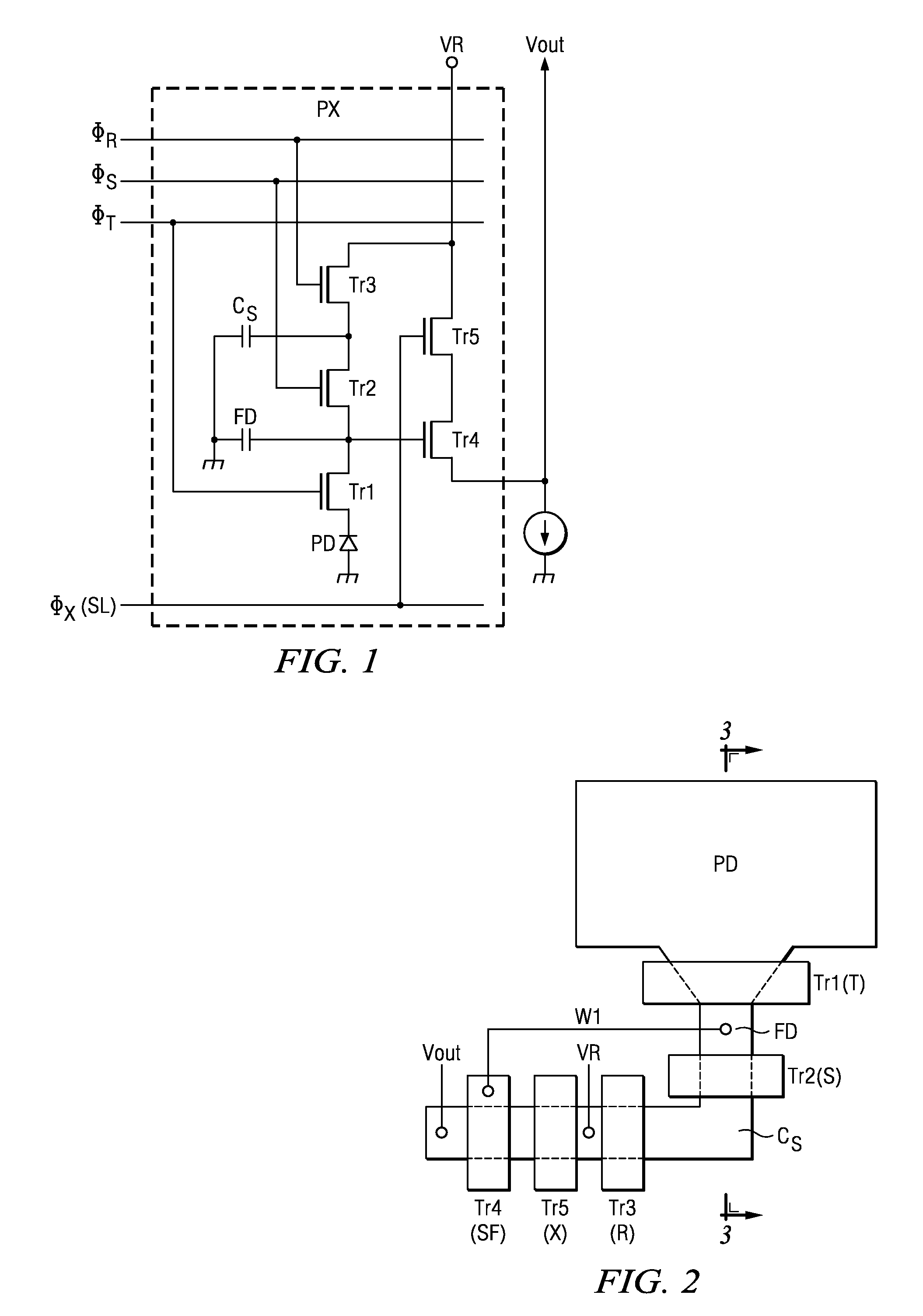
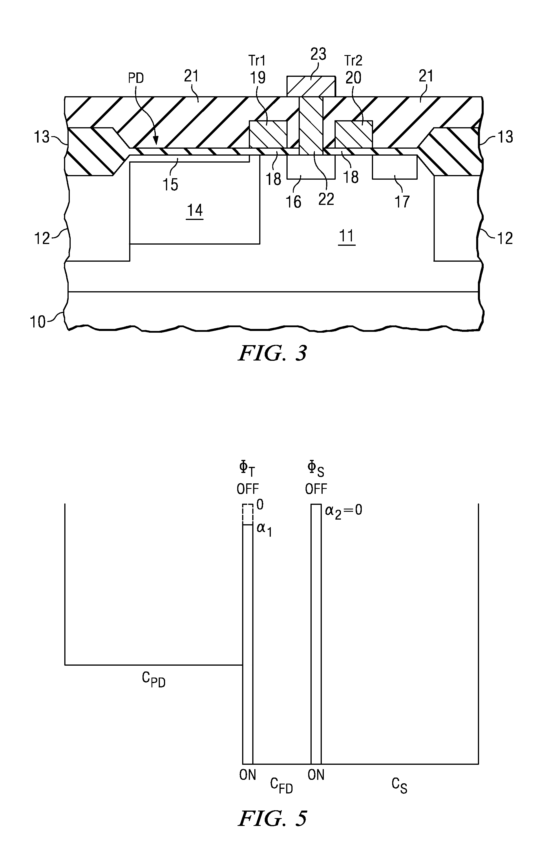
[0041]The solid-state image pickup device pertaining to the present embodiment is a CMOS image sensor. FIG. 1 is an equivalent circuit diagram illustrating one pixel PX (pixel).

[0042]For a so-called five-transistor type CMOS image sensor, each pixel includes the following elements: a photodiode PD which receives light and generates and stores photoelectric charge; a transfer transistor Tr1 which transfers such photoelectric charge from such photodiode PD; a floating diffusion FD which transfers such photoelectric charge through such transfer transistor Tr1; an additive capacitive element Cs; a capacitive coupling transistor Tr2 which combines or divides the capacitance of such floating diffusion FD and the capacitance of such additive capacitive element Cs; a reset transistor Tr3 which is connected to floating diffusion FD and exhausts the photoelectric charge in floating diffusion FD; an amplifying transistor Tr4 (source follower SF) that amplifies and converts the photoelectric ch...

second embodiment

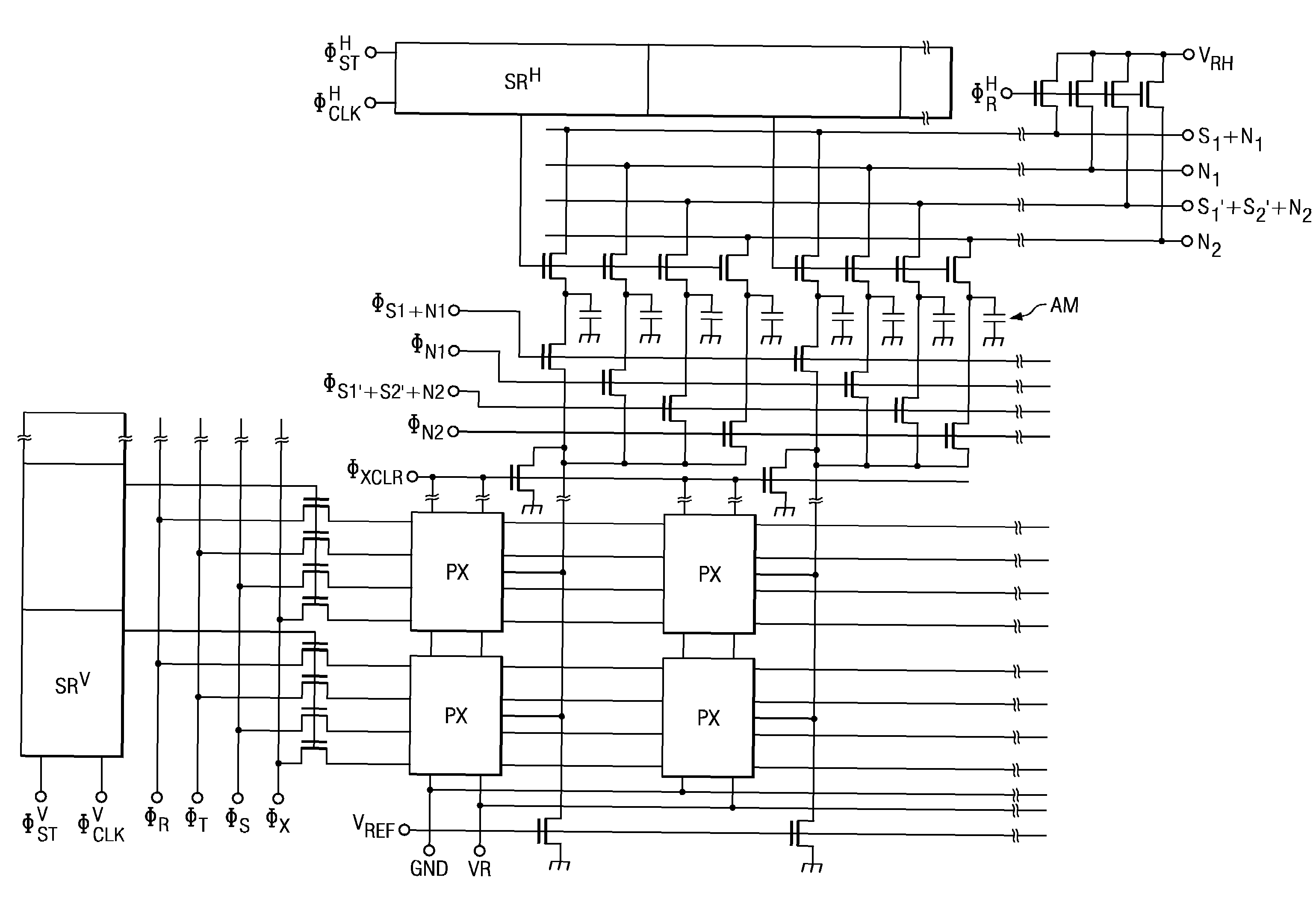
[0071]FIG. 10 is an equivalent circuit diagram illustrating a portion of eight pixels of a CMOS image sensor as the solid-state image pickup device in a second embodiment. While the CMOS image sensor in the first embodiment is a so-called five-transistor type CMOS image sensor having five transistors for each pixel: a transfer transistor, capacitive coupling transistor, reset transistor, amplifying transistor (source follower), and selecting transistor Tr5, the present embodiment has a configuration in which the reset transistor and additive capacitive element are shared by four pixels adjacent to each other in the vertical direction (V direction).

[0072]As shown in FIG. 10, in the vertical direction (V direction), lines 1-4 are set side-by-side, and, in the horizontal direction, columns 1-2 are set side-by-side. Eight pixels are set in this configuration. Pixels have photodiodes PD11-PD14, PD21-PD24, and floating diffusions FD11-FD14, FD21-FD24, respectively. Also, transfer transist...

third embodiment

[0075]FIG. 12 is an equivalent circuit diagram illustrating a portion of eight pixels of a CMOS image sensor as the solid-state image pickup device of a third embodiment. Just as in the second embodiment, the reset transistor and the additive capacitive element are shared by four pixels that are adjacent in the vertical direction (V direction), and, in addition, the selecting transistor is shared by two pixels that are adjacent in the horizontal direction (H direction).

[0076]As shown in FIG. 12, in the vertical direction (V direction), lines 1-4 are set side-by-side, and, in the horizontal direction, columns 1-2 are set side-by-side. Eight pixels are set in this configuration. The pixels have photodiodes PD11-PD14, PD21-PD24, and floating diffusions FD11-FD14, FD21-FD24, respectively. Also, transfer transistor T, capacitive coupling transistor S, and an amplifying transistor (source follower) are set for each pixel. Here, the four pixels adjacent to each other in the vertical direct...


PUM


Abstract

The invention provides a solid-state image pickup device and method for realizing a higher sensitivity and a higher S/N ratio especially in the low-luminance region while maintaining a wide dynamic range. Plural pixels are integrated in an array configuration on a semiconductor substrate with each pixel having photodiode PD, which receives light and generates and stores photoelectric charge, transfer transistor Tr1, which transfers such photoelectric charge from such photodiode, floating diffusion FD, which transfers such photoelectric charge through such transfer transistor, additive capacitive element Cs, which is set connected via the floating diffusion to the photodiode, capacitive coupling transistor Tr2, which combines or divides the capacitance of such floating diffusion and the capacitance of such additive capacitive element, and reset transistor Tr3, which is connected to such additive capacitive element or floating diffusion; and the capacitance of the floating diffusion is smaller than that of the photodiode.

Description

[0001]This application claims priority from Japanese Patent Application No. 2007-036978, filed 16 Feb. 2007.FIELD OF THE INVENTION[0002]This relates to solid-state image pickup devices and methods.BACKGROUND[0003]The demand for image input image sensors, such as CMOS (complementary metal-oxide-semiconductor) image sensors or CCD (charge coupled device) image sensors, in the application fields of digital cameras and cellular phones equipped with cameras, has increased along with the performance improvement of such image sensors. Image sensors with improved performance characteristics are desired. One such characteristic is expansion of the dynamic range. For such image sensors, further improvement in characteristics is demanded, and one of the characteristics is the dynamic range that should be expanded.[0004]Examples of solid-state image pickup devices designed for realizing a wider dynamic range are given in Japanese Kokai Patent Application No. 2003-134396, Japanese Kokai Patent A...

Claims


Application Information

Patent Timeline
Patent Type & Authority Applications(United States)
IPC IPC(8): H01L27/146H04N5/335H04N5/355H04N5/369H04N5/374H04N5/376
CPCH01L27/14609H01L27/14643H01L27/14641H04N5/3559H04N5/3743H04N3/155H04N25/59H04N25/768H04N25/771
Inventor OSHIKUBO, HIROMICHIADACHI, SATORU
Owner TEXAS INSTR INC
Why Eureka
Try Eureka