

Semiconductor memory device, semiconductor device, memory system and refresh control method
a memory device and semiconductor technology, applied in the direction of information storage, static storage, digital storage, etc., can solve the problems of limited holding area of common banks, and achieve the effect of reducing the current consumption of the pasr and maximizing the cache capacity
- Summary
- Abstract
- Description
- Claims
- Application Information
AI Technical Summary
Benefits of technology
Problems solved by technology
Method used
Image

Examples
Embodiment Construction
[0043]A preferred embodiment of the present invention will be described with reference to the accompanying drawings. In the embodiment, a case of applying the present invention to a DRAM having a configuration for performing a self refresh operation for a memory cell array divined into a plurality of banks will be described.
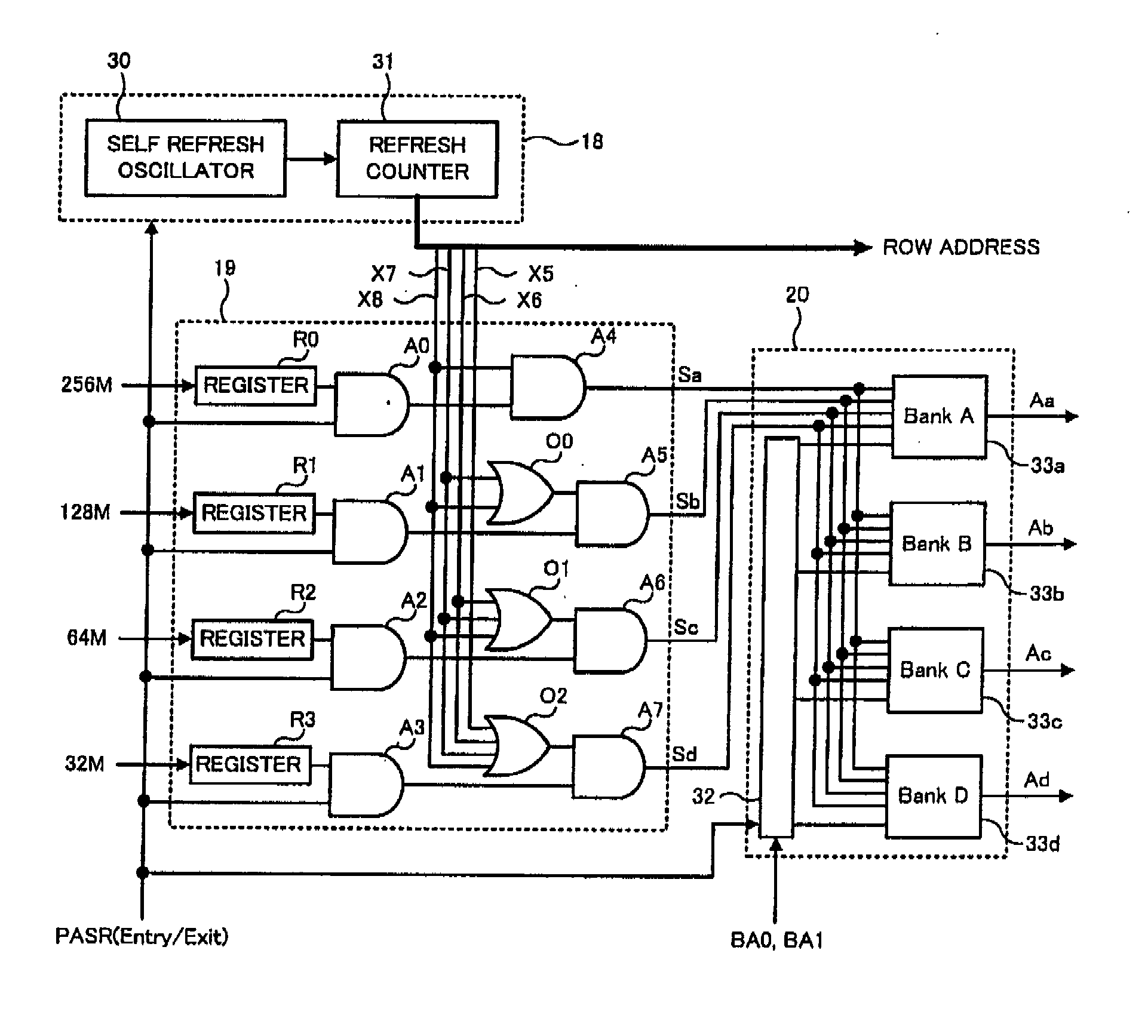
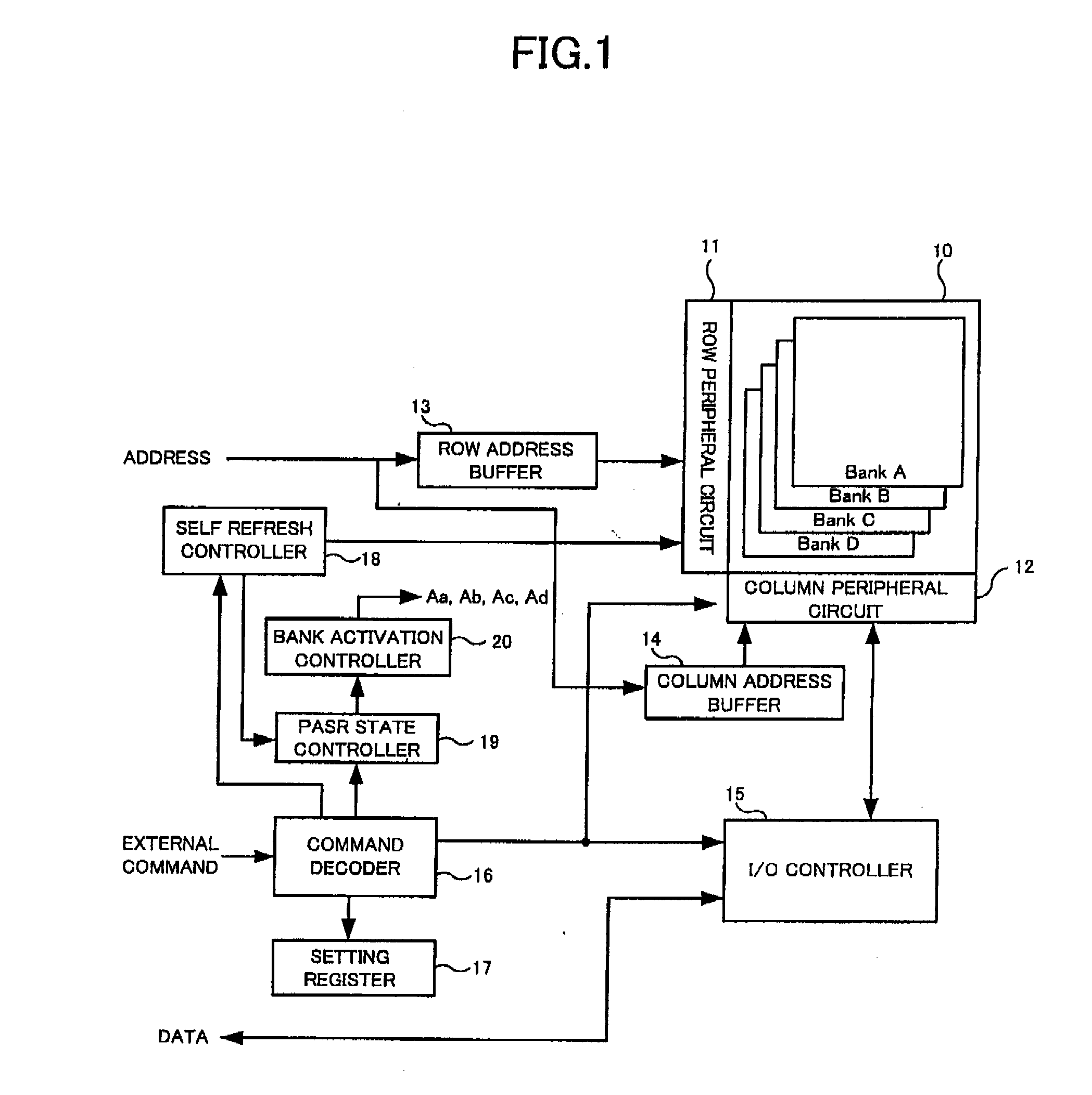
[0044]FIG. 1 is a block diagram showing a schematic entire configuration of the DRAM of the embodiment. This embodiment exemplifies a DRAM having an entire storage capacity of 512 Mbits and having a four bank configuration. The DRAM as shown in FIG. 1 includes a memory cell array 10, a row peripheral circuit 11, a column peripheral circuit 12, a row address buffer 13, a column address buffer 14, an I / O controller 15, a command decoder 16, a setting register 17, a self refresh controller 18, a PASR state controller 19, and a bank activation controller 20.
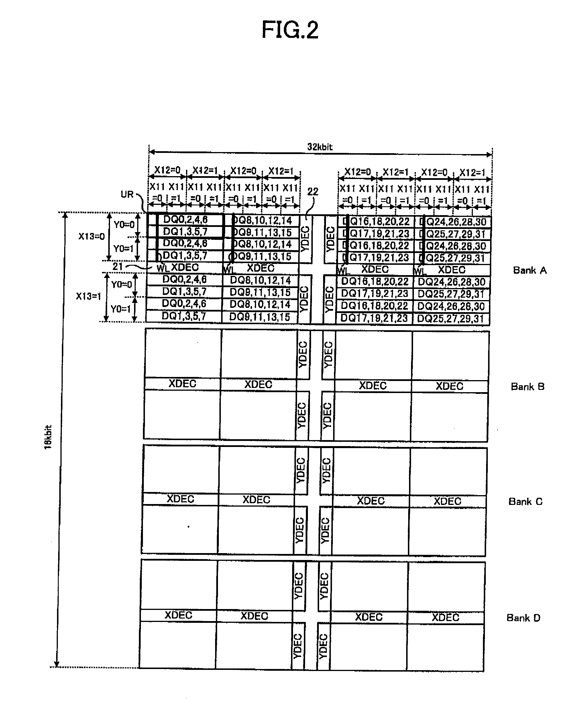
[0045]The memory cell array 10 is divided into four banks A, B, C and D, and each bank has the same storage cap...
PUM
 Abstract
Description
Claims
Application Information