Semiconductor device

a technology of semiconductors and components, applied in the direction of burglar alarm mechanical actuation, burglar alarm by hand-portable articles removal, instruments, etc., can solve the problems of production cost increase, and difficult to provide an inexpensive rf tag

Inactive Publication Date: 2008-09-04
SEMICON ENERGY LAB CO LTD
View PDF11 Cites 23 Cited by
  • Summary
  • Abstract
  • Description
  • Claims
  • Application Information

AI Technical Summary

Benefits of technology

[0021]According to the present invention, a high-performance RF tag which can electrically rewrite data such as ID data after production can be provided at a low price.

Problems solved by technology

In addition, since a high voltage is necessary for writing in a flash memory, a special booster circuit is necessary, and it is difficult to provide an inexpensive RF tag.
Furthermore, since the number of processes increases, production cost increases and it is further difficult to provide an inexpensive RF tag.
However, since data of the mask ROM is determined in a production process and data rewriting is incapable after production, convenience of the RF tag is to be lost.

Method used


Image

  • Semiconductor device
  • Semiconductor device
  • Semiconductor device

Examples


embodiment mode 1

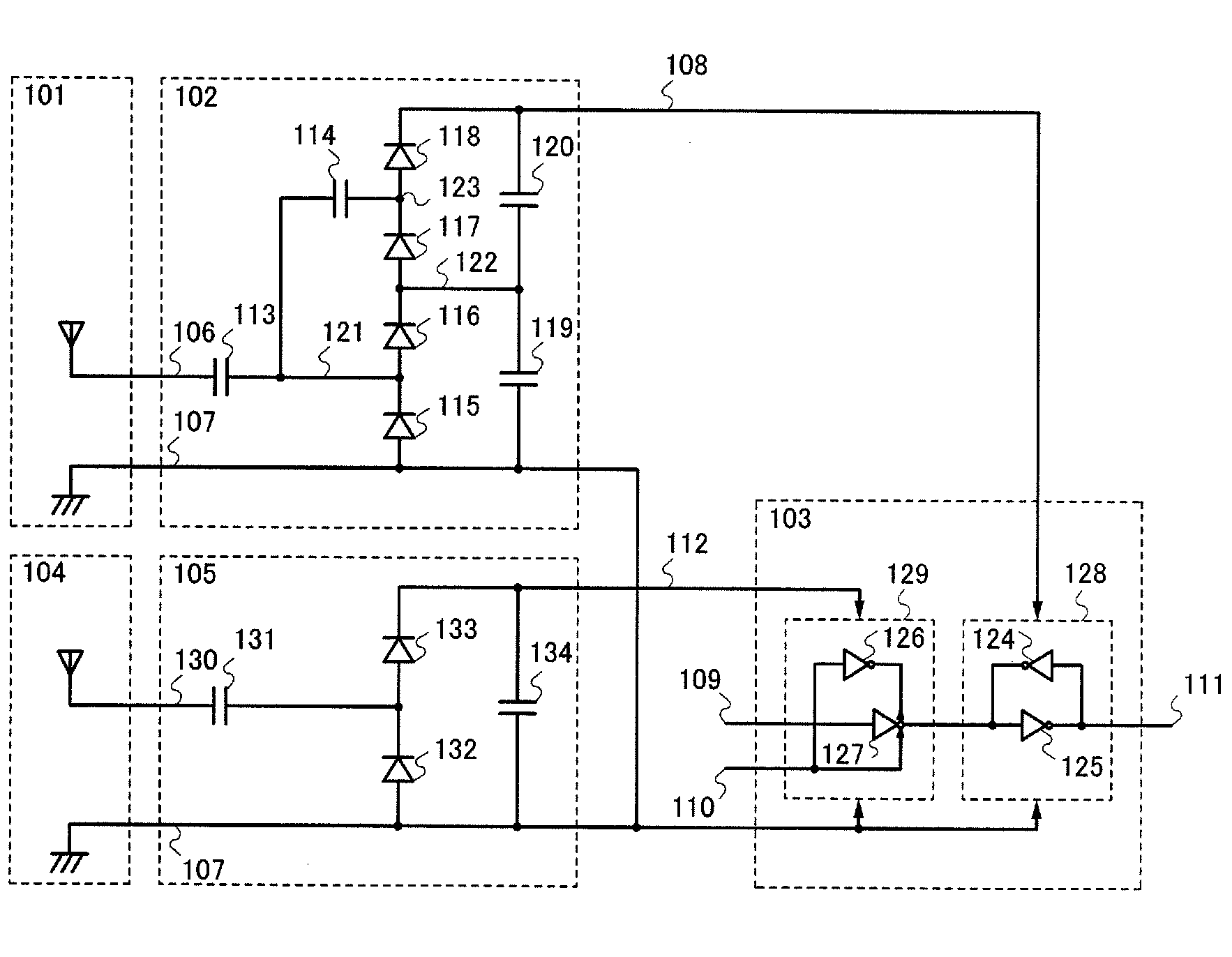
[0029]Embodiment Mode 1 in which a power supply circuit and a memory circuit to be mounted on an RF tag of the present invention will be described with reference to FIG. 1. FIG. 1 is a circuit diagram of the power supply circuit and the memory circuit to be mounted on the RF tag of the present invention. In FIG. 1, there are a first antenna circuit 101, a first power supply circuit 102, a memory circuit 103, a second antenna circuit 104, and a second power supply circuit 105.

[0030]The first antenna circuit 101 has a function to generate a first alternating voltage between a first antenna input wiring 106 and a ground wiring 107 when the first antenna circuit 101 receives a first weak radio signal. Specifically, for example, the above function can be realized as long as the first antenna circuit 101 has a coil in the case where an electromagnetic induction method is used for receiving a first communication signal, or the above function can be realized as long as the first antenna cir...

embodiment mode 2

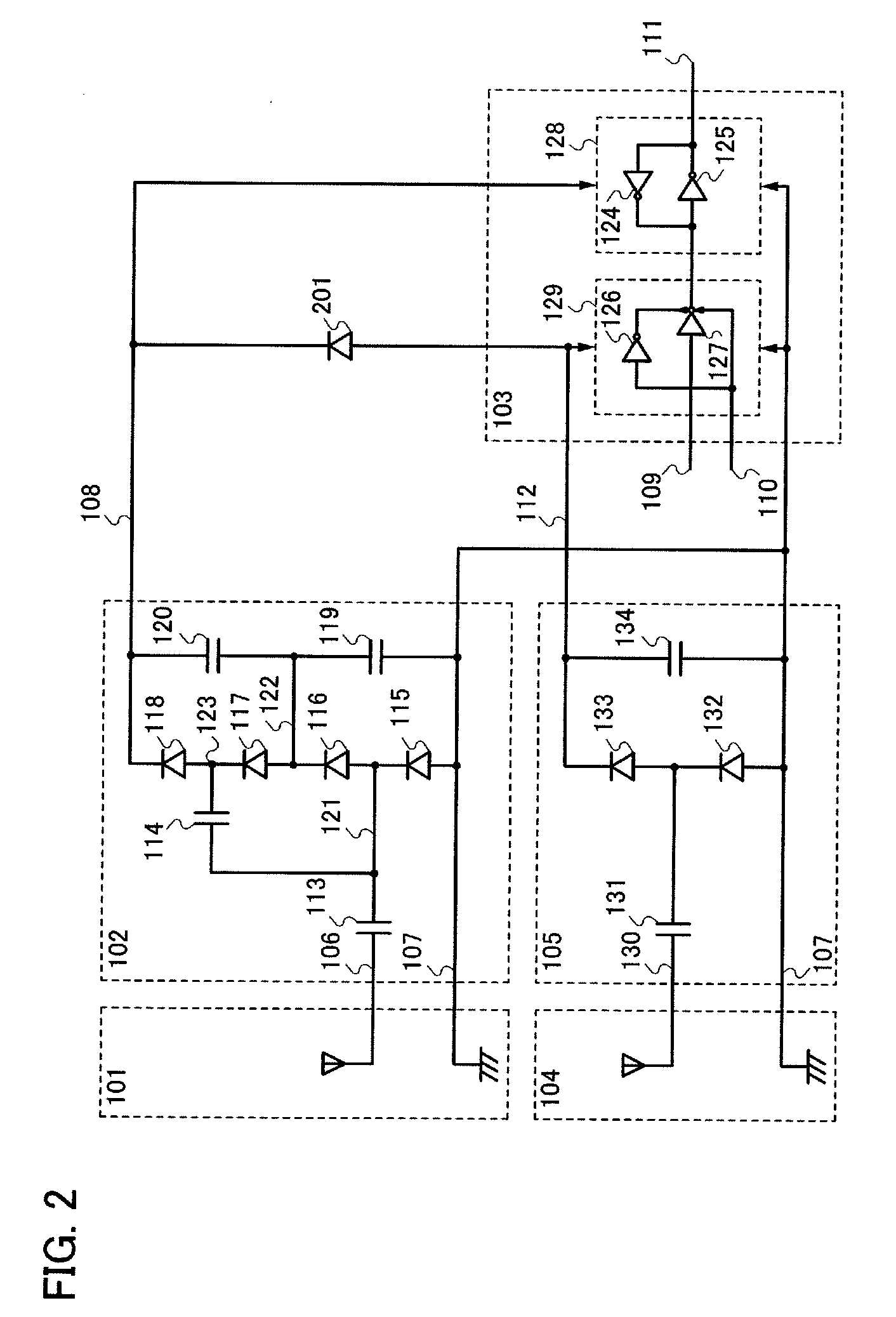
[0046]Embodiment Mode 2 which is different from Embodiment Mode 1 where the power supply circuits and the memory circuit 103 are mounted on the RF tag of the present invention will be described with reference to FIG. 2. FIG. 2 is a circuit diagram of the power supply circuit and the memory circuit 103 which are mounted on the RF tag of the present invention.

[0047]In FIG. 2, the first antenna circuit 101, the first power supply circuit 102, the memory circuit 103, the second antenna circuit 104, and the second power supply circuit 105 can be described in much the same way as in FIG. 1 in Embodiment Mode 1. FIG. 2 is different from FIG. 1 described in Embodiment Mode 1 in that a diode 201 is inserted between the second power source wiring 112 and the first power source wiring 108.

[0048]The function of the diode 201 is as follows. That is, when a potential of the second power source wiring 112, namely, the second power supply voltage is higher than the potential of the first power sour...

embodiment 1

[0055]Hereinafter, embodiments of the present invention will be described with reference to the accompanying drawings. However, the present invention can be implemented in various modes. As can be easily understood by a person skilled in the art, the modes and details of the present invention can be changed in various ways without departing from the spirit and scope of the present invention. Thus, the present invention should not be interpreted as being limited to the following description of the embodiments. Through the drawings of the embodiments, the same components or components having the same functions are denoted by the same reference numerals and will not be further explained.

[0056]An embodiment in which a power supply circuit to be mounted on the RF tag of the present invention will be described with reference to FIGS. 3A and 3B. FIGS. 3A and 3B each are a circuit diagram of the power supply circuit to be mounted on the RF tag of the present invention.

[0057]In FIG. 3A, the ...


PUM


Abstract

In an RF tag, a mask ROM or a flash memory is used for storing data such as an ID number. Although the mask ROM can be realized at a low price, rewriting is not possible. In addition, in the flash memory, although electric rewriting is possible, production cost increases. Accordingly, it is difficult to provide an RF tag by which data rewriting is possible at a low price. An RF tag is provided with a power supply circuit having a function to generate a power supply voltage from a weak radio signal and a memory which can hold data stored in a data holding portion by the power supply voltage. With the above structure, a high-performance RF tag capable of rewriting data such as an ID number after production can be provided at a low price.

Description

BACKGROUND OF THE INVENTION[0001]1. Field of the Invention[0002]The present invention relates to a semiconductor device which transmits and receives data by a radio signal.[0003]2. Description of the Related Art[0004]In recent years, a compact semiconductor device (hereinafter, an RF tag) that is a combination of an ultra compact IC chip and an antenna for wireless communication has received a lot of attention. The RF tag is known as an information medium which incorporates a semiconductor memory and which can read information stored in the semiconductor memory or can write information in the semiconductor device by radio waves from a wireless communication device (hereinafter, a reader / writer).[0005]For example, an RF tag in which a communication circuit, a signal control circuit, and a memory portion are formed in a semiconductor integrated circuit and they are combined with an antenna is disclosed (e.g., refer to Patent Document 1).[0006]As an application field of the RF tag, mer...

Claims


Application Information

Patent Timeline
Patent Type & Authority Applications(United States)
IPC IPC(8): H04B7/00H01Q11/12
CPCG06K19/0723G06K19/07767H02M7/103H02J17/00G11C5/142H02J50/10H02J50/27H02J50/40
Inventor KUROKAWA, YOSHIYUKI
Owner SEMICON ENERGY LAB CO LTD
Why Eureka
Try Eureka