Semiconductor acceleration sensor

a technology of acceleration sensor and semiconductor, applied in the direction of speed/acceleration/shock measurement, semiconductor devices, instruments, etc., can solve the problems of significant degradation of sensitivity in the x- and y-axis directions compared to that in the z-axis direction sensor sensitivity degradation, etc., to achieve the effect of mass production of sensors with stable characteristics and reduced mass

Inactive Publication Date: 2008-09-11
LAPIS SEMICON CO LTD
View PDF3 Cites 10 Cited by
  • Summary
  • Abstract
  • Description
  • Claims
  • Application Information

AI Technical Summary

Benefits of technology

[0017]According to the present invention, since a second mass portion having a higher specific gravity is connected beneath a first mass portion composed of a semiconductor substrate, the thickness of the mass can be reduced without degrading the sensor sensitivity. Furthermore, since the second mass portion can be formed by means of semiconductor fabricating technologies including photolithography, positional shift between the first and the second mass portions can be suppressed and the mass production of sensors with stable characteristics is enabled.

Problems solved by technology

This, however, reduces the mass of the mass, which may lead to the degradation of sensitivity of the sensor.
Reduction in the thickness of mass, in particular, leads to significant degradation of sensitivity in the X- and Y-axis directions compared to that in the Z-axis direction.
This means that reducing the thickness of the mass 18 degrades sensitivity in the X- and Y-directions to be increased more than that in the Z-axis direction, thereby causing the problem of unbalanced sensitivity between the Z-axis direction and the X- and Y-axis directions.
However, this causes a problem of increasing the size of the sensor 10 itself.

Method used


Image

  • Semiconductor acceleration sensor
  • Semiconductor acceleration sensor
  • Semiconductor acceleration sensor

Examples


Embodiment Construction

[0036]In the following detailed description of the preferred embodiments, reference is made to the accompanying drawings which form a part hereof, and in which is shown by way of illustration specific preferred embodiments in which the inventions may be practiced. These preferred embodiments are described in sufficient detail to enable those skilled in the art to practice the invention, and it is to be understood that other preferred embodiments may be utilized and that logical, mechanical and electrical changes may be made without departing from the spirit and scope of the present inventions. The following detailed description is, therefore, not to be taken in a limiting sense, and scope of the present inventions is defined only by the appended claims.

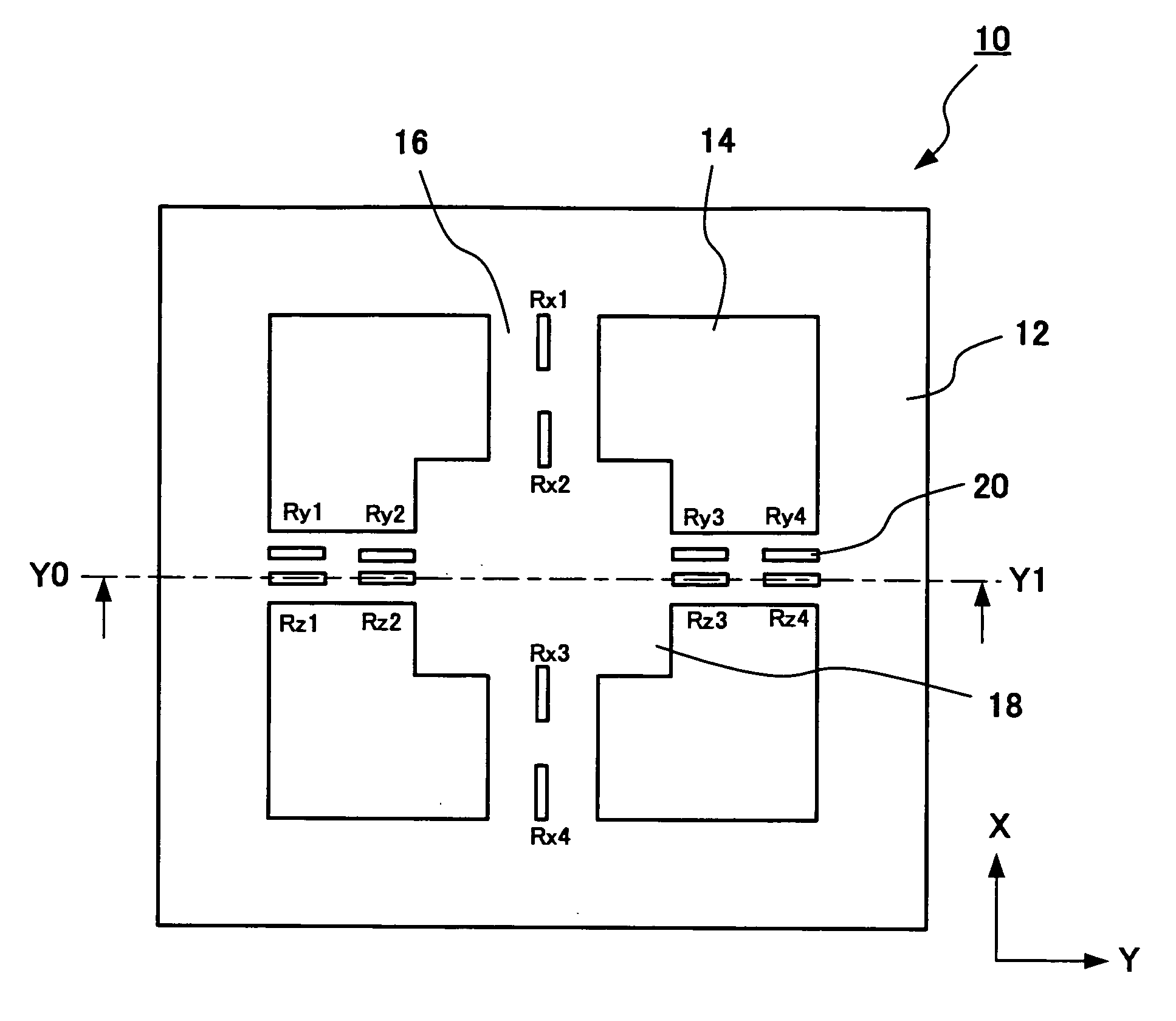
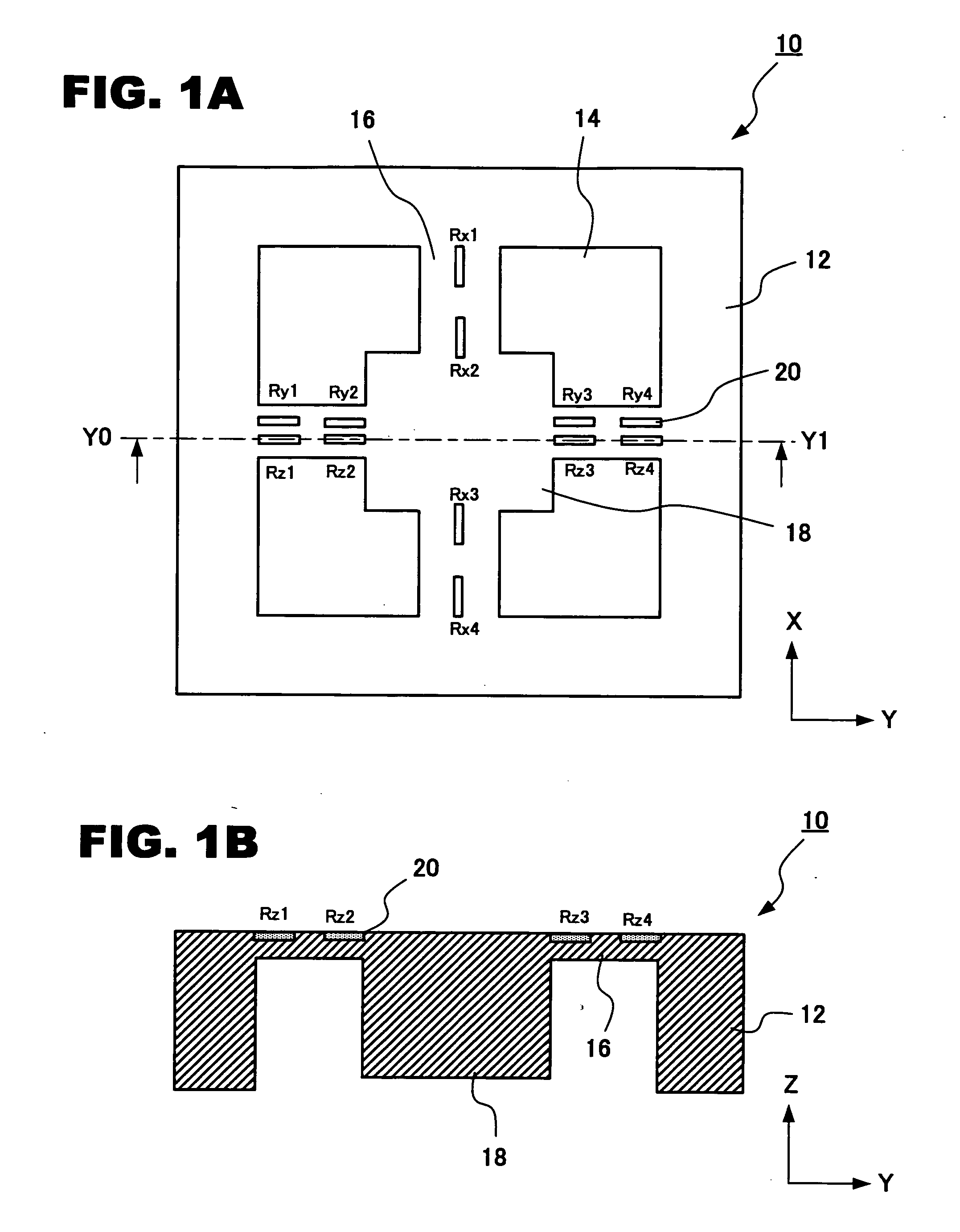
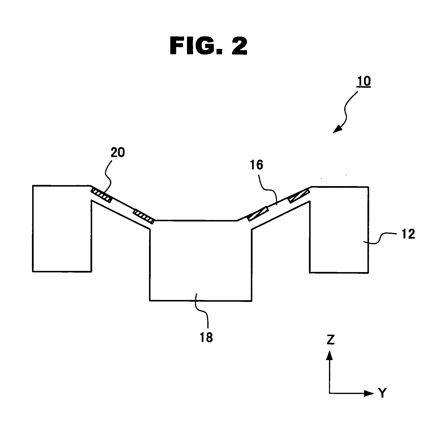
[0037]FIGS. 6A and 6B are schematic diagrams of a three-dimensional semiconductor acceleration sensor showing an embodiment of the present invention. An acceleration sensor 110 is composed of a semiconductor substrate and fabricated b...


PUM


Abstract

According to the present invention, a semiconductor acceleration sensor fabricated using a semiconductor substrate comprises: an outer frame formed by the semiconductor substrate; a plurality of beam portions formed by the semiconductor substrate and connected to the outer frame; a first mass portion formed by the semiconductor substrate and connected to the beam portion; and a second mass portion connected to the end face opposite to the beam portion of the first mass portion. The second mass portion is formed of material having a higher specific gravity than the first mass portion.

Description

CROSS REFERENCE TO RELATED APPLICATION[0001]This application claims the priority of Application No. 2007-060149, fled Mar. 9, 2007 in Japan, the subject matter of which is incorporated herein by reference.TECHNICAL FIELD OF THE INVENTION[0002]The present invention relates to a semiconductor acceleration sensor fabricated using a semiconductor substrate, and its fabricating method.BACKGROUND OF THE INVENTION[0003]A semiconductor sensor detects acceleration by detecting variations in resistance value of piezo resistors that are caused when a flexible section bends due to the change of the position of a mass portion supported by the flexible section in which the piezo resistors are formed. Such a semiconductor sensor is used for measuring acceleration such as that of a running automobile in the running or lateral direction or camera shake of a camcorder.[0004]A conventional three-dimensional acceleration sensor utilizing piezo resistance detection system capable of detecting accelerati...

Claims


Application Information

Patent Timeline
Patent Type & Authority Applications(United States)
IPC IPC(8): G01P15/12G01P15/18H01L29/84
CPCG01P15/18G01P15/123G01P2015/084
Inventor KATOU, KENJI
Owner LAPIS SEMICON CO LTD
Why Eureka
Try Eureka