Quantum dot sensitized wide bandgap semiconductor photovoltaic devices & methods of fabricating same

a wide bandgap, quantum dot technology, applied in semiconductor/solid-state device manufacturing, semiconductor devices, electrical equipment, etc., can solve the problem of reducing the efficiency of solar conversion of such devices to 10%, reducing the qd content of semiconductor heterojunction photovoltaic devices, and reducing the qd content of semiconductor heterojunction devices.

Inactive Publication Date: 2008-09-11
SEAGATE TECH LLC
View PDF38 Cites 67 Cited by
  • Summary
  • Abstract
  • Description
  • Claims
  • Application Information

AI Technical Summary

Benefits of technology

[0014]An advantage of the present invention is an improved quantum dot (QD) sensitized wide bandgap (WBG) semiconductor heterojunction photovoltaic (PV) device.
[0015]Another advantage of the present invention is an improved quantum dot (QD) sensitized wide bandgap (WBG) semiconductor heterojunction photovoltaic (PV) device with an active PV layer having a substantially increased QD content.
[0016]Still another advantage of the present invention is an improved quantum dot (QD) sensitized wide bandgap (WBG) semiconductor heterojunction photovoltaic (PV) device with dual-sided irradiation capability.
[0017]Yet another advantage of the present invention is an improved method of fabricating quantum dot (QD) sensitized wide bandgap (WBG) semiconductor heterojunction photovoltaic (PV) devices.
[0018]A further advantage of the present invention is an improved method of fabricating quantum dot (QD) sensitized wide bandgap (WBG) semiconductor heterojunction photovoltaic (PV) devices with active PV layers having substantially increased QD content.
[0019]A still further advantage of the present invention is an improved method of fabricating quantum dot (QD) sensitized wide bandgap (WBG) semiconductor heterojunction photovoltaic (PV) devices with dual-sided irradiation capability.

Problems solved by technology

Disadvantageously, however, this results in greater opportunity for loss of excited electron-hole pairs (“excitons”) due to recombination and thermalization.
Consequently, the efficiency of solar conversion of such devices is generally limited to ˜10%.
Notwithstanding the potential for increased photon conversion efficiency afforded by the solid state heterojunction QD-sensitized PV cells such as described above, the heretofore utilized manufacturing techniques comprising absorption of the QD material from solution onto a porous body of a WBG semiconductor material, as well as in situ processing, result in relatively low surface-to-volume ratios of the WBG semiconductor particles (e.g., TiO2), which when combined with the relatively low coverage of the WBG particle surfaces with QD's, limits the actual performance and viability of such devices.

Method used


Image

  • Quantum dot sensitized wide bandgap semiconductor photovoltaic devices & methods of fabricating same
  • Quantum dot sensitized wide bandgap semiconductor photovoltaic devices & methods of fabricating same
  • Quantum dot sensitized wide bandgap semiconductor photovoltaic devices & methods of fabricating same

Examples


Embodiment Construction

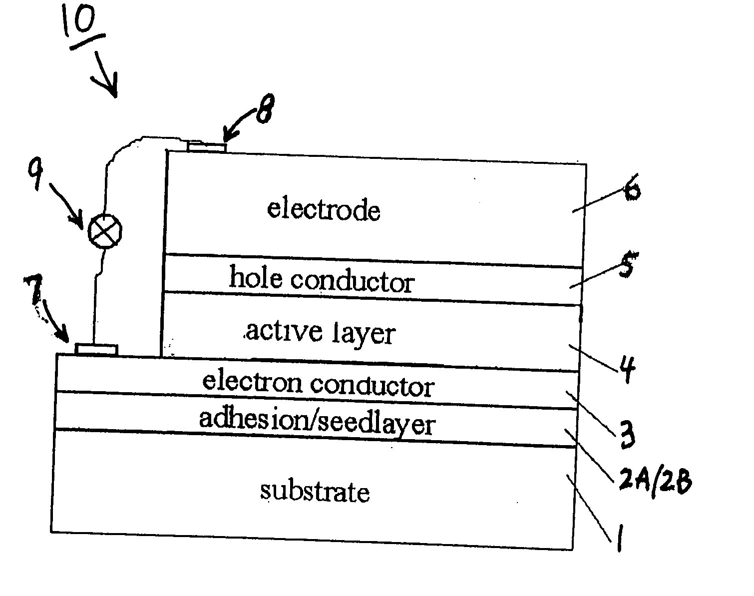
[0075]The present invention is based upon recognition that solid-state heterojunction QD-sensitized PV cells can be fabricated with substantially improved viability when used as solar energy-to-electrical energy conversion devices than heretofore possible via conventional methodologies, including absorption of the QD material from colloidal solution and in situ processing. According to the present invention, the active photovoltaic layer of solid-state heterojunction QD-sensitized PV cells is a novel granular film structure comprising a columnar-shaped, 2-dimensional matrix including a substantially greater volume (hence amount) of QD material, relative to WBG material, than heretofore afforded by the aforementioned conventional methodologies, such as absorption of QD material from solution and in situ processing.

[0076]More specifically, according to the present invention, a substrate (preferably transparent) with an electrically conductive granular layer thereon (e.g., transparent ...


PUM


Abstract

A quantum dot (QD) sensitized wide bandgap (WBG) semiconductor heterojunction photovoltaic (PV) device comprises an electron conductive layer; an active photovoltaic (PV) layer adjacent the electron conductive layer; a hole conductive layer adjacent the active PV layer; and an electrode layer adjacent the hole conductive layer. The active PV layer comprises a wide bandgap (WBG) semiconductor material with Eg≧2.0 eV, in the form of a 2-dimensional matrix defining at least two open spaces, and a narrower bandgap semiconductor material with Eg<2.0 eV, in the form of quantum dots (QD's) filling each open space defined by the matrix of WBG semiconductor material and establishing a heterojunction therewith. The active PV layer is preferably fabricated by a co-sputter deposition process, and the QD's constitute from about 40 to about 90 vol. % of the active PV layer.

Description

FIELD OF THE INVENTION[0001]The present invention relates to improved quantum dot sensitized wide bandgap semiconductor photovoltaic devices and methods for fabricating same. The invention has particular utility in the manufacture and use of photovoltaic solar cells for direct conversion of radiant to electrical energy.BACKGROUND OF THE INVENTION[0002]A recently developed class of photovoltaic (“PV”) cells and devices, sometimes referred to as “Graetzel Cells” (see, e.g., U.S. Pat. Nos. 4,684,537; 5,350,644; 5,463,057; 5,525,440; and 6,278,056 B1), is based upon dye-sensitization of a wide bandgap (“WBG”) semiconductor (i.e., Eg≧2 eV, preferably ≧3 eV), such as TiO2, for efficient injection of electrons into the conduction band upon photo-excitation of the dye molecules, followed by charge separation and photovoltage generation utilizing a liquid electrolyte for hole conduction. While such devices are attractive in terms of their inherent simplicity and use of environmentally stable...

Claims


Application Information

Patent Timeline
Patent Type & Authority Applications(United States)
IPC IPC(8): H01L31/04H01L21/02
CPCH01L31/0352H01L31/0324Y02E10/50H01L31/06
Inventor HARKNESS, SAMUEL D.RICHTER, HANS J.
Owner SEAGATE TECH LLC
Why Eureka
Try Eureka