

Active device array substrate
a technology of active devices and array substrates, which is applied in the direction of semiconductor devices, instruments, electrical equipment, etc., can solve the problems of reducing the mura effect, affecting the quality of the display panel, and removing as many defects as are detectable, so as to achieve the effect of reducing or eliminating the mura
- Summary
- Abstract
- Description
- Claims
- Application Information
AI Technical Summary
Benefits of technology
Problems solved by technology
Method used
Image



Examples
first embodiment
[0029]FIGS. 1A and 1B are schematic top views showing the process of fabricating an active device array substrate according to one embodiment of the present invention. FIGS. 2A through 2D are schematic cross-sectional views along section line I-I′ of FIGS. 1A and 1B showing the process of fabricating an active device array substrate according to one embodiment of the present invention.
[0030]First, as shown in FIGS. 1A and 2A, the method of fabricating the active device array substrate in the present invention includes providing a substrate 100. Then, a plurality of scan lines 102, a plurality of data lines 104 and a plurality of active devices 106 are formed over the substrate 100. Each of the active devices 106 is electrically connected to the corresponding scan line 102 and data line 104. The active devices 106 are, for example, thin film transistors comprising a gate electrode 106a, a gate insulation layer 106b, a channel layer 106c, a source 106d and a drain 106e. The gate elect...
second embodiment
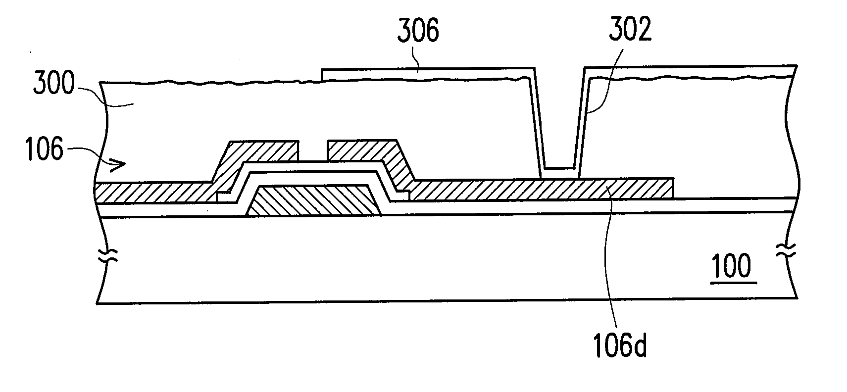
[0036]In the first embodiment, the active device array substrate is formed with a protective layer under the organic material layer. However, the protective layer is not absolutely essential in the present invention. In fact, the organic material layer can be directly formed after forming the active devices, the data lines and the scan lines. In the following, a detailed description is provided.
[0037]FIGS. 3A through 3D are schematic cross-sectional views showing the process of fabricating an active device array substrate according to a second embodiment of the present invention. As shown in FIG. 3A, the method of fabricating the active device array substrate in the present invention includes providing a substrate 100. Then, a plurality of scan lines 102, a plurality of data lines 104 and a plurality of active devices 106 are formed over the substrate 100. Each of the active devices 106 is electrically connected to the corresponding scan line 102 and data line 104.
[0038]As shown in ...
PUM
 Abstract
Description
Claims
Application Information