Semiconductor Light emitting device, LED package using the same, and method for fabricating the same

Inactive Publication Date: 2008-09-11
STANLEY ELECTRIC CO LTD
View PDF12 Cites 45 Cited by
  • Summary
  • Abstract
  • Description
  • Claims
  • Application Information

AI Technical Summary

Benefits of technology

[0023]The present invention as described above can prevent the reflectance of a metal film (being a reflection layer) from deteriorating due to heat aging. The present invention can also prevent wire bonding performance of the semico

Problems solved by technology

When this occurs, the Ag crystalline particles adversely coarsen with ease.
However, adding another element cannot perfectly prevent the decrease in reflectance due to heat.
Even when an Ag alloy is used to form a reflection layer of an LED light emitting device, repeated operations can significantly decrease the reflectance of the Ag alloy, thereby causing po

Method used


Image

  • Semiconductor Light emitting device, LED package using the same, and method for fabricating the same
  • Semiconductor Light emitting device, LED package using the same, and method for fabricating the same
  • Semiconductor Light emitting device, LED package using the same, and method for fabricating the same

Examples


Example

FIRST EXAMPLE

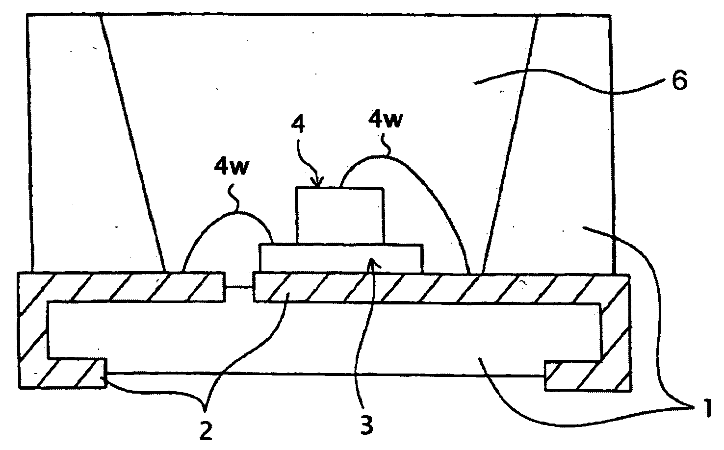
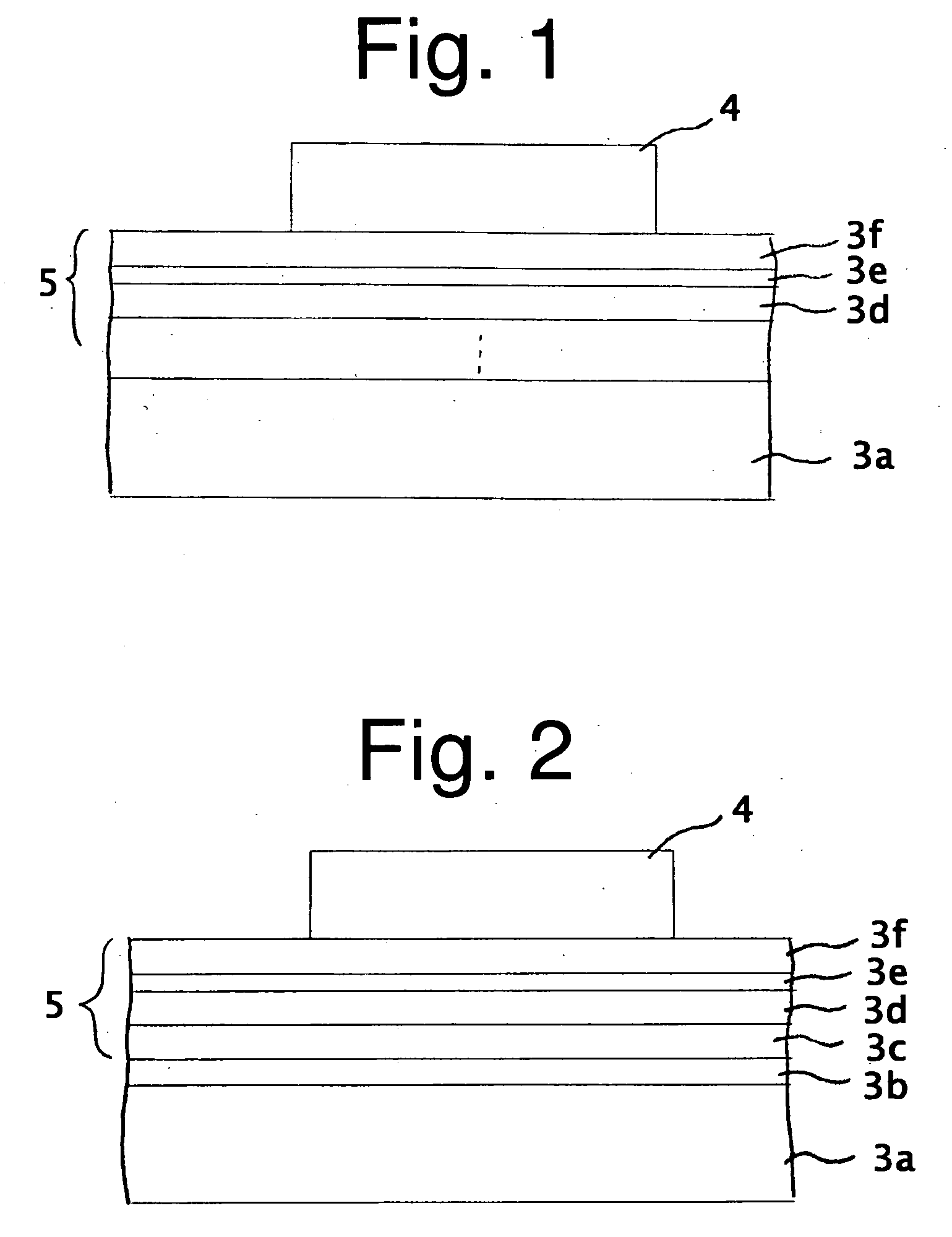
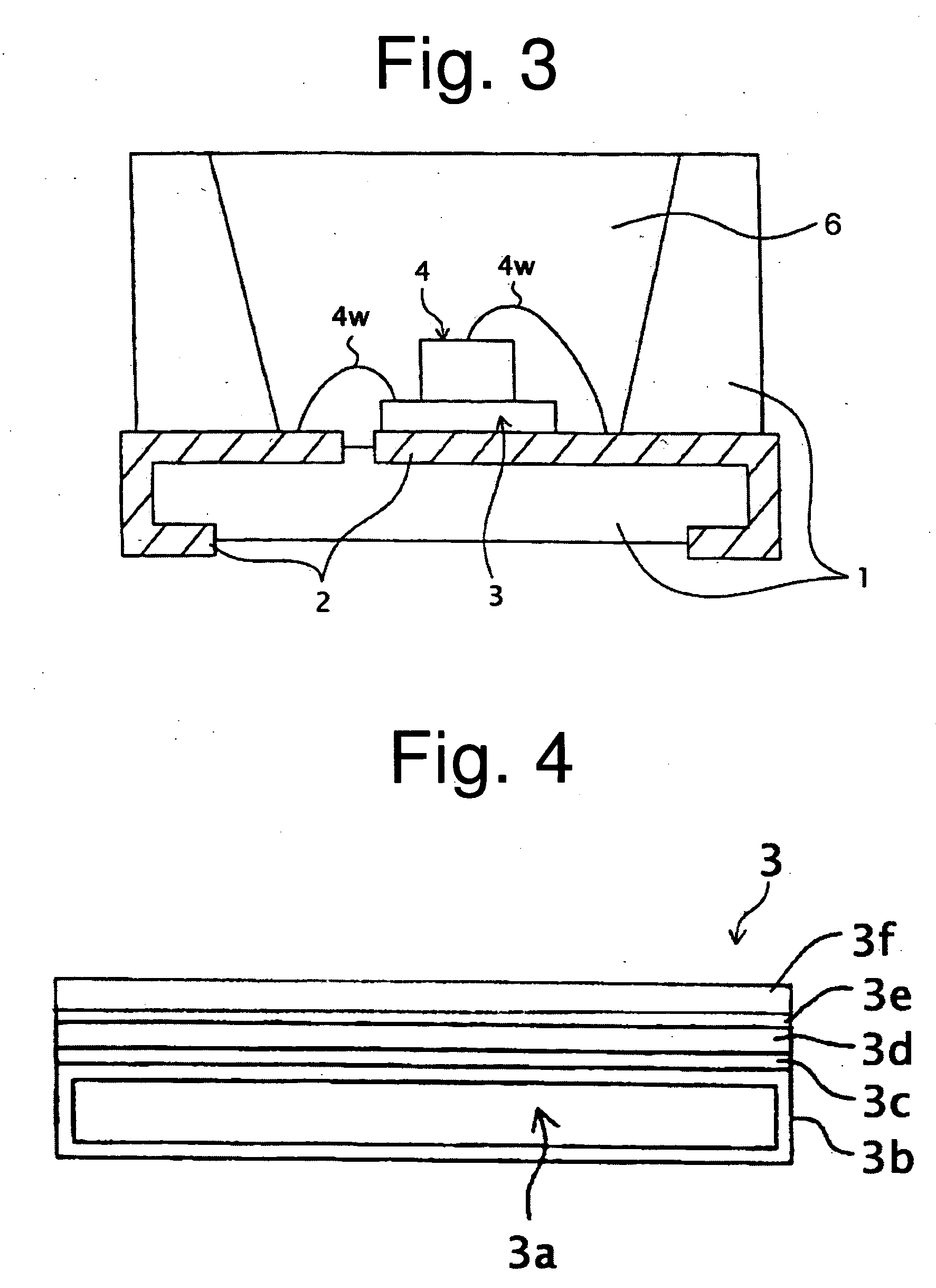
[0080]In the first example, a metal film 5 was deposited on a flat silicon substrate with an oxide film. Its reflectance was measured before and after a heat aging test.

[0081]Specifically, the films were deposited on the silicon substrate with an oxide film under the following deposition conditions. A Ti film serving as an adhesion layer 3c was formed with an argon pressure of 1 Pa and a DC output of 1 kW to have a thickness of 75 nm. A Ni film serving as a barrier metal layer 3d was formed with an argon pressure of 0.2 Pa and a DC output of 1 kW to have a thickness of 250 nm. A Ti film serving as a metal layer 3e was formed with an argon pressure of 0.2 Pa and a DC output of 1 kW to have a thickness of from 0.35 to 300 nm (in particular, samples were prepared having the Ti film at thicknesses indicated by the data points in FIGS. 10 and 11, including 0.35 nm, 1 nm, 50 nm, 100 nm, 150 nm, 200 nm and 300 nm). (A control sample without a metal layer 3e was also prepared a...

Example

SECOND EXAMPLE

[0084]In the second example, a metal film 5 was deposited on a flat silicon substrate with an oxide film. Its reflectance was measured before and after the heat aging test.

[0085]Specifically, the films were deposited on the silicon substrate with an oxide film under the following deposition conditions. A Ti film serving as an adhesion layer 3c was formed with an argon pressure of 1 Pa and a DC output of 1 kW to have a thickness of 75 nm. A Ni film serving as a barrier metal layer 3d was formed with an argon pressure of 0.2 Pa and a DC output of 1 kW to have a thickness of 250 nm. A Pd film serving as a metal layer 3e was formed with an argon pressure of 0.2 Pa and a DC output of 500 W to have a thickness of from 1 to 1000 nm (in particular, samples were prepared having the Pd film at thicknesses indicated by the data points in FIGS. 12 and 13, including 1 nm, 100 nm, 300 nm, 500 nm and 1000 nm). (A control sample without a metal layer 3e was also prepared and is indica...

Example

THIRD EXAMPLE

[0089]In the third example, a metal film was deposited on a flat silicon substrate with an oxide film. The substrate was then wire-bonded and subjected to a pulling-strength test.

[0090]Specifically, the films were deposited on the silicon substrate with an oxide film under the following deposition conditions. A Ti film serving as an adhesion layer 3c was formed with an argon pressure of 1 Pa and a DC output of 1 kW to have a thickness of 75 nm. A Ni film serving as a barrier metal layer 3d was formed with an argon pressure of 0.2 Pa and a DC output of 1 kW to have a thickness of 250 nm. A Ti film serving as a metal layer 3e was formed with an argon pressure of 0.2 Pa and a DC output of 1 kW to have a thickness of from 0.35 to 300 nm (in particular, samples were prepared having the Ti film at thicknesses indicated by the data points in FIG. 14, including 0.35 nm, 20 nm, 50 nm, 100 nm and 300 nm). (A control sample without a metal layer 3e was also prepared and is indicat...


PUM


Abstract

A semiconductor light emitting device is provided which can prevent the reflectance of a metal film from deteriorating due to heat aging and can prevent wire bonding performance of the semiconductor light emitting element from deteriorating due to the diffusion of Ni contained in a Ni barrier metal layer to the reflection layer during die-bonding of the semiconductor light emitting element. The semiconductor light emitting device includes a metal film formed on a substrate and a semiconductor light emitting element. The metal film includes a barrier metal layer configured to prevent a predetermined material from being diffused into the substrate, a metal layer formed on the barrier metal layer; and a reflection layer formed on the metal layer. The reflection layer is configured to reflect light emitted from the semiconductor light emitting element, and the metal layer is made of Ti or Pd.

Description

[0001]This application claims the priority benefit under 35 U.S.C. §119 of Japanese Patent Application No. 2007-058644 filed on Mar. 8, 2007, which is hereby incorporated in its entirety by reference.BACKGROUND OF THE INVENTION[0002]1. Field of the Invention[0003]The present invention to a semiconductor light emitting device, an LED package using the same, and a method for fabricating the same.[0004]2. Description of the Related Art[0005]Conventionally, semiconductor light emitting devices using an LED as a light emitting element are now used prevailingly. In such a device, the optical output efficiency and durability are required to be improved further. As an example of a semiconductor light emitting device, an LED package is disclosed in Japanese patent application Laid-Open No. 2005-277380 (corresponding to U.S. Application Publication No. US 2006 / 0001055 A1, both of which are hereby incorporated by reference in their entireties). The LED package has a horn formed by anisotropica...

Claims


Application Information

Patent Timeline
IPC IPC(8): H01L33/00H01L21/00H01L33/56H01L33/60H01L33/62
CPCH01L33/405H01L33/60H01L2924/10253H01L2224/45144H01L2224/48091H01L2924/00014H01L2924/00H01L2924/19107H01L2224/16225
Inventor SUZUKI, NAOTONAKAMURA, YOSHIHIROYASUDA, YOSHIAKI
Owner STANLEY ELECTRIC CO LTD
Why Eureka
Try Eureka