Optical waveguide element and optical waveguide device

Pending Publication Date: 2022-05-26
SUMITOMO OSAKA CEMENT CO LTD
View PDF0 Cites 2 Cited by
  • Summary
  • Abstract
  • Description
  • Claims
  • Application Information

AI Technical Summary

Benefits of technology

[0021]According to the present invention, in an optical waveguide element using a thinly processed substrate such as a rib-type optical modulation element, it is possible t

Problems solved by technology

However, as a result of thinly processing the substrate to a thickness of several μm or less, a new problem may occur.
That is, in an optical waveguide element such as an optical modulation element that uses an optical waveguide formed on a substrate, generally, an optical coupling portion between an optical fiber for light input and an optical waveguide, a light branching section such as a Y-branch waveguide, and/or a curved waveguide portion where a propagation direction of light changes, light propagating in the optical waveguide may leak into the substrate and become unnecessary light.
Such unnecessary light is reflected in the substrate and the

Method used


Image

  • Optical waveguide element and optical waveguide device
  • Optical waveguide element and optical waveguide device
  • Optical waveguide element and optical waveguide device

Examples


first embodiment

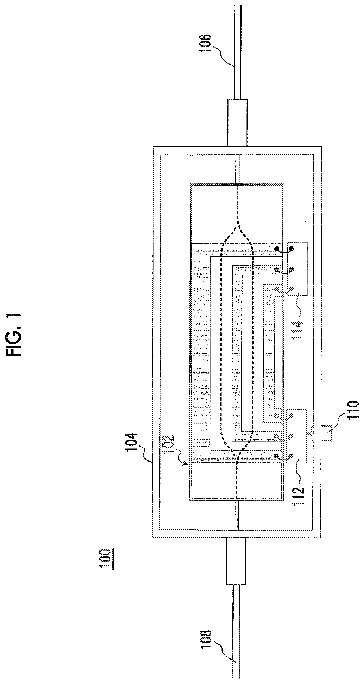
[0035]FIG. 1 is a diagram illustrating a configuration of an optical waveguide element and an optical waveguide device according to a first embodiment of the present invention. In the present embodiment, the optical waveguide element is an optical modulation element 102 that performs optical modulation by using a Mach-Zehnder optical waveguide, and the optical waveguide device is an optical modulation device 100 that uses the optical modulation element 102.

[0036]The optical modulation device 100 houses the optical modulation element 102 inside a housing 104. A cover (not illustrated) which is a plate body is finally fixed to an opening of the housing 104, and the inside of the housing 104 is airtightly sealed.

[0037]The optical modulation device 100 further includes an input optical fiber 106 for inputting light into the housing 104, and an output optical fiber 108 for guiding light modulated by the optical modulation element 102 to the outside of the housing 104.

[0038]The optical mo...

second embodiment

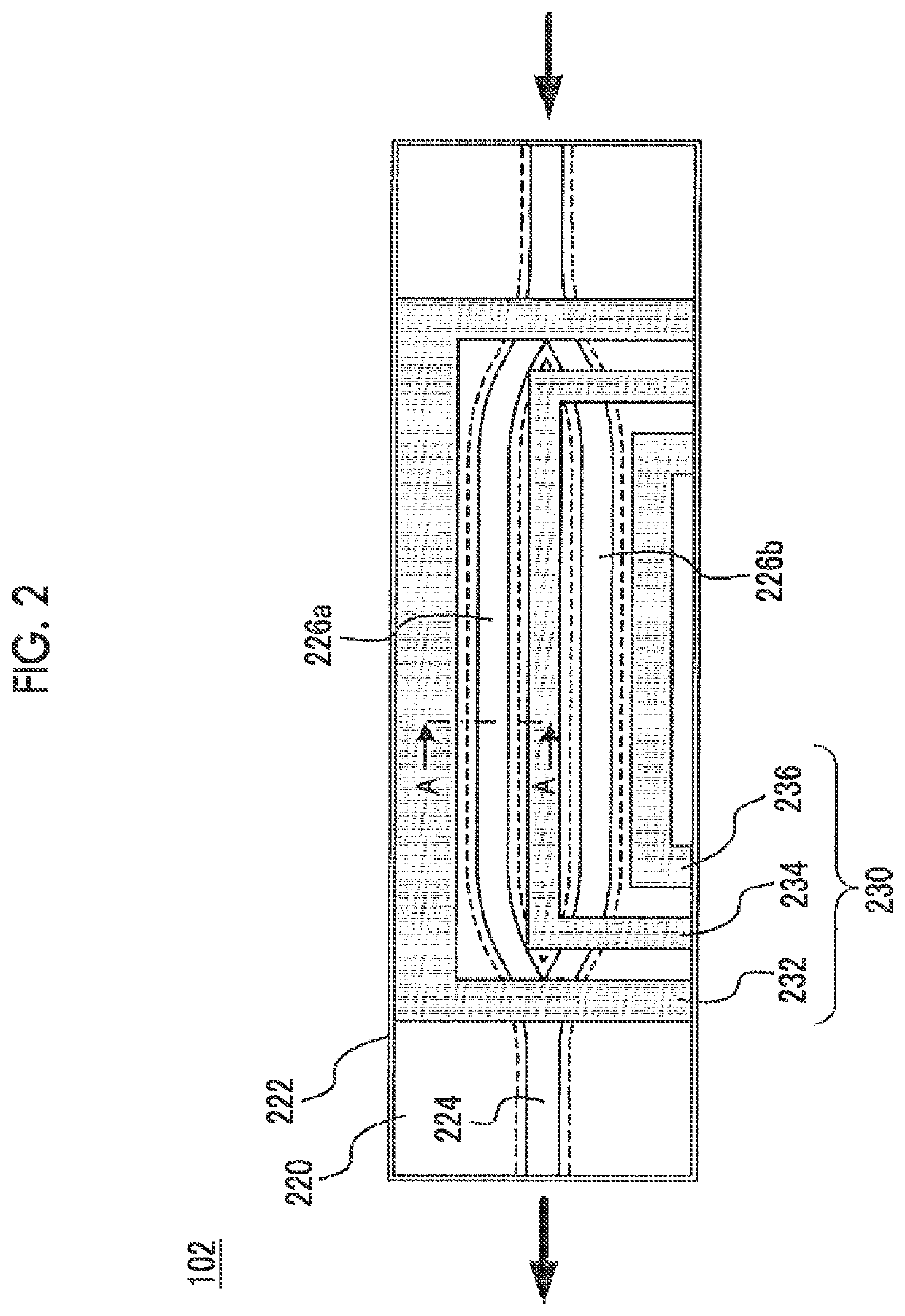
[0064]Next, a second embodiment of the present invention will be described. FIGS. 9, 10, and 11 are diagrams illustrating the configurations of an optical modulation element 802 that is an optical waveguide element according to the second embodiment of the present invention, and an optical modulation device 800 that is an optical waveguide device using the same.

[0065]In FIGS. 9, 10, and 11, the same reference numerals as those in FIGS. 1, 2, and 3 are used for the same constituents as those in FIGS. 1, 2 and 3 as described above, and the description of FIGS. 1, 2 and 3 will be incorporated.

[0066]The optical modulation device 800 illustrated in FIG. 9 has the same configuration as the optical modulation device 100 except that the optical modulation element 802 is used instead of the optical modulation element 102. In the optical modulation device 800, the optical modulation element 802 is different from the optical modulation device 100 in that the optical modulation element 802 has ...


PUM


Abstract

In an optical waveguide element, performance deterioration due to recoupling of unnecessary light leaking from an optical waveguide with the optical waveguide is prevented. An optical waveguide element includes an optical substrate on which an optical waveguide is formed, and a support substrate that is bonded to the optical substrate, on a bonded surface of the support substrate bonded to the optical substrate, a recess portion along the optical waveguide on the optical substrate is formed directly under the optical waveguide, a portion of the support substrate from an upper surface of the support substrate to at least a depth of a bottom surface of the recess portion has a refractive index higher than a substrate refractive index of the optical substrate, and the recess portion is filled with a substance having a refractive index lower than the substrate refractive index.

Description

TECHNICAL FIELD[0001]The present invention relates to an optical waveguide element that is a functional element using an optical waveguide, such as an optical modulation element, and an optical waveguide device using such an optical waveguide element.BACKGROUND ART[0002]In high-speed / large-capacity optical fiber communication systems, optical transmission apparatuses incorporating a waveguide type optical modulator are often used. Above all, an optical modulation element using LiNbO3 (hereinafter, also referred to as LN) having an electro-optic effect for a substrate has low light loss and can realize a wide-band optical modulation characteristic compared with an optical modulation element using a semiconductor-based material such as indium phosphide (InP), silicon (Si), or gallium arsenide (GaAs), and is thus widely used in high-speed / large-capacity optical fiber communication systems.[0003]On the other hand, in a modulation method in an optical fiber communication system, multi-le...

Claims


Application Information

Patent Timeline
IPC IPC(8): G02B6/125G02F1/035G02F1/21G02F1/225G02B6/122
CPCG02B6/125G02F1/0356G02B2006/12142G02F1/2255G02B6/1223G02F1/212G02F1/035G02F1/01
Inventor KUGIMOTO, YUKIMIYAZAKI, NORIKAZUKATAOKA, YU
Owner SUMITOMO OSAKA CEMENT CO LTD
Why Eureka
Try Eureka