Ultra-thin soi CMOS with raised epitaxial source and drain and embedded sige pfet extension

a technology of embedded pfet extension and epitaxial source, which is applied in the field of forming ultrathin soi (utsoi) field effect transistors, can solve the problems of incorporating stress into utsoi fets, and none of this prior art addresses the integration of embedded pfet sige extension with raised source/drain regions, so as to improve pfet device extension and channel region conductivity, reduce contact and source/

Inactive Publication Date: 2008-09-11
IBM CORP +1
View PDF5 Cites 83 Cited by
  • Summary
  • Abstract
  • Description
  • Claims
  • Application Information

AI Technical Summary

Benefits of technology

[0009]The present invention provides a novel semiconductor device structure that includes integrating embedded PFET devices with a SiGe extension with raised CMOS source drain regions. Particularly, according to the invention, epitaxially grown raised source and drain structures are formed to reduce contact and source / drain resistance. Additionally, implemented are the embedded SiGe extensions to improve the PFET device extension and channel region conductivity.

Problems solved by technology

Incorporating stress into UTSOI FETs is a challenge because of the thin channel region.
None of this prior art however, addresses the integration of an embedded pFET SiGe extension with raised source / drain regions.

Method used


Image

  • Ultra-thin soi CMOS with raised epitaxial source and drain and embedded sige pfet extension
  • Ultra-thin soi CMOS with raised epitaxial source and drain and embedded sige pfet extension
  • Ultra-thin soi CMOS with raised epitaxial source and drain and embedded sige pfet extension

Examples


Embodiment Construction

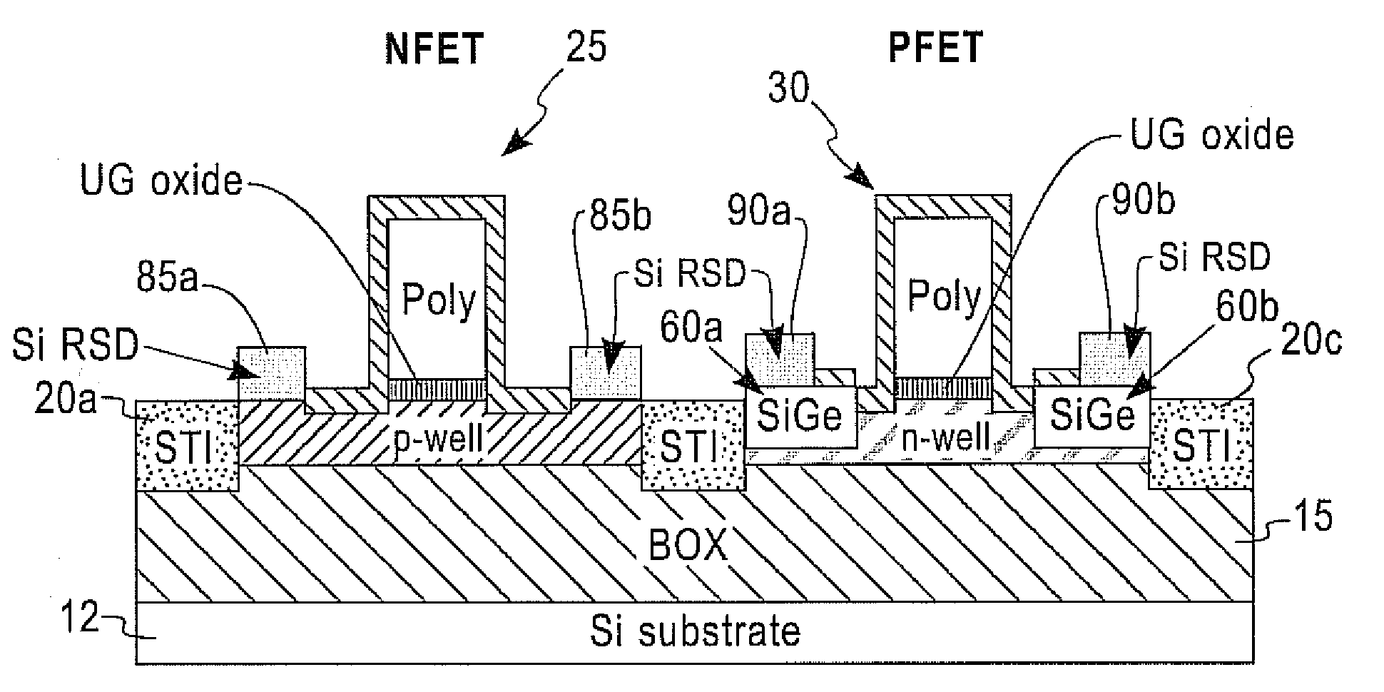
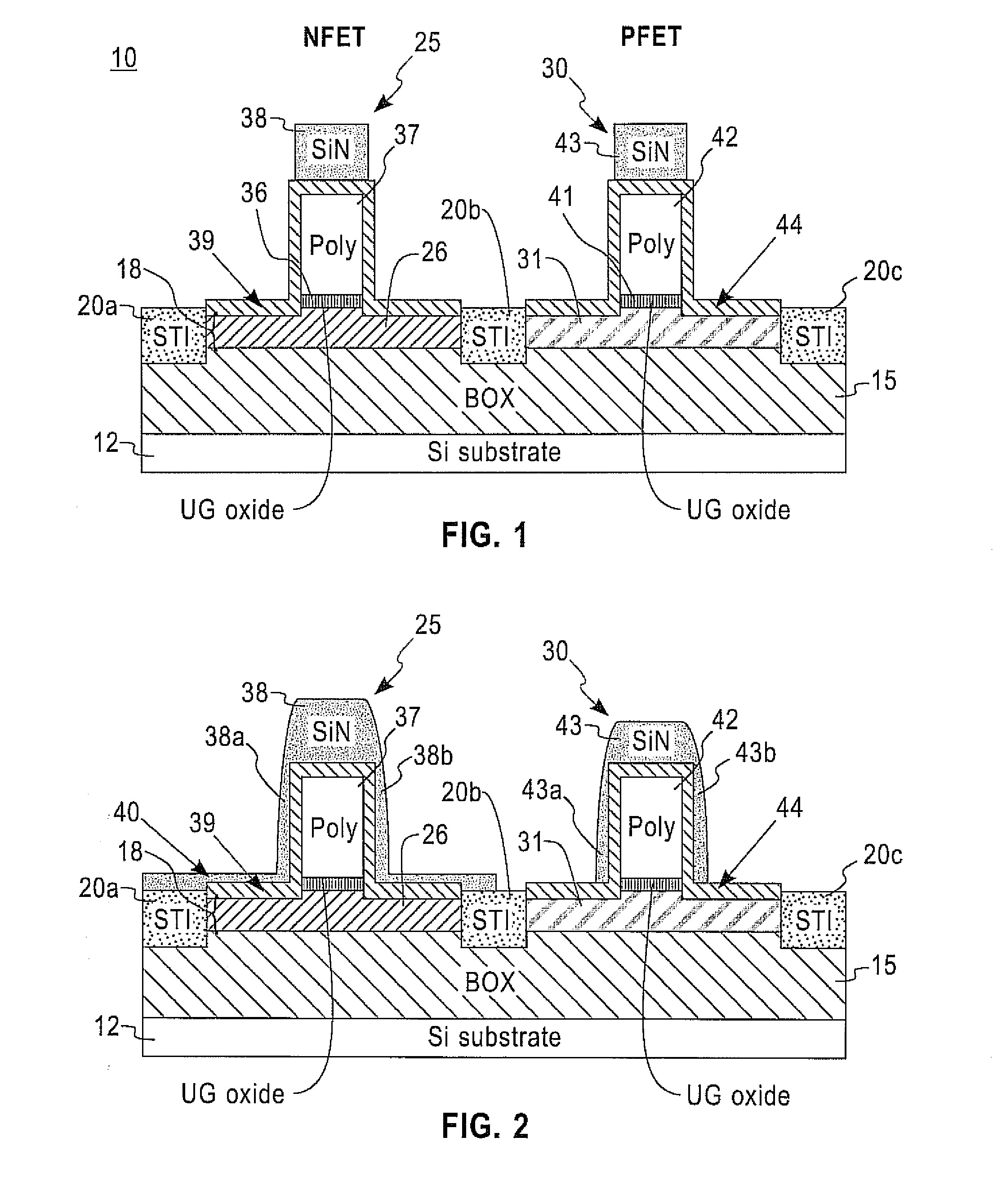
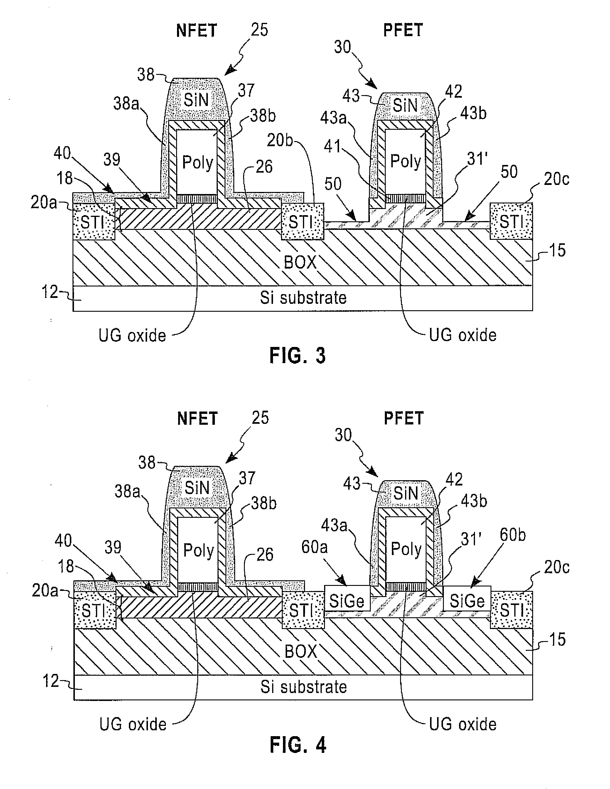
[0038]The present invention is directed to a method for forming ultra-thin SOI (UTSOI) field effect transistors with stressed channel regions that provide increased carrier mobility.

[0039]FIG. 1 shows, through cross-sectional view, a semiconductor structure 10 resulting from conventional UTSOI processing. As shown, in FIG. 1, there is first fabricated an SOI structure including a buried oxide (BOX) region 15 (e.g., an oxide, nitride, oxynitride or any combination thereof, with an oxide such as SiO2 being most typical) that is located between a top Si-containing layer 18 and a bottom Si-containing layer 12. Preferably, the BOX region 15 is continuous. The thickness of the BOX region 15 formed in the present invention may vary depending upon the exact embodiments and conditions used in fabricating the same. Typically, however, the BOX region has a thickness from about 200 to about 1800 Å, with a BOX thickness from about 1300 to about 1600 Å being more typical.

[0040]Insofar as the top ...


PUM


Abstract

A method for improving channel carrier mobility in ultra-thin Silicon-on-oxide (UTSOI) FET devices by integrating an embedded pFET SiGe extension with raised source/drain regions. The method includes selectively growing embedded SiGe (eSiGe) extensions in pFET regions and forming strain-free raised Si or SiGe source/drain (RSD) regions on CMOS. The eSiGe extension regions enhance hole mobility in the pFET channels and reduce resistance in the pFET extensions. The strain-free raised source/drain regions reduce contact resistance in both UTSOI pFETs and nFETs.

Description

FIELD OF THE INVENTION [0001]The present invention related generally to the fabrication of complementary metal oxide semiconductor (CMOS) field effect transistors (FET), and more particularly, to a method for forming ultra-thin SOI (UTSOI) field effect transistors with stressed channel regions which provide increased carrier mobility among other benefits.BACKGROUND OF THE INVENTION [0002]CMOS FETs are employed in almost every electronic circuit application such as signal processing, computing, and wireless communications. It has been demonstrated that ultra-thin SOI (UTSOI) FETs have a very good short channel control due to extremely thin channel region. Thin body devices however, lead to high series resistance Rext, which can be mitigated by forming raised source / drain (RSD) regions. It has also been demonstrated however, that thick channel SOI FETs exhibit improved FET performance such as switching speed and drive current, by applying stress in the channel. The improvement stems f...

Claims


Application Information

Patent Timeline
Patent Type & Authority Applications(United States)
IPC IPC(8): H01L21/8238
CPCH01L21/823807H01L21/823814H01L21/823878H01L29/7848H01L27/1203H01L29/6653H01L29/66636H01L21/84
Inventor MAJUMDAR, AMLANPEI, GENREN, ZHIBINSINGH, DINKARSLEIGHT, JEFFREY W.
Owner IBM CORP
Why Eureka
Try Eureka