Fabrication method of a mixed substrate and use of the substrate for producing circuits

a technology of mixed substrates and circuits, which is applied in the direction of basic electric elements, semiconductor/solid-state device manufacturing, electrical equipment, etc., can solve the problems of strain relaxation, defects, and defects, and achieve the effect of reducing the defect rate of the substrate and being simple to perform

Active Publication Date: 2008-09-11
COMMISSARIAT A LENERGIE ATOMIQUE ET AUX ENERGIES ALTERNATIVES
View PDF11 Cites 13 Cited by
  • Summary
  • Abstract
  • Description
  • Claims
  • Application Information

AI Technical Summary

Benefits of technology

[0014]The object of the invention is to remedy all the above-mentioned drawbacks and has the object of providing a fabrication method of a mixed substrate which enables a tensile strain to be induced on a silicon-on-insulator portion of the substrate and a compressive strain to be induced on a germanium-on-insulator portion of the substrate, a method which is simple to perform while at the same time achieving a maximum reduction of the defect rate of the substrate.

Problems solved by technology

The germanium enrichment technique on a silicon-on-insulator SOI substrate therefore presents a technical limitation, i.e. relaxation of the strains and the appearance of defects during enrichment.
This approach therefore does not enable the two germanium and silicon channels to be obtained on the same plane and therefore does not enable very thin silicon layers to be obtained, which are in particular interesting for fully depleted technologies to reduce short channel effects.
However, such a technique does not enable a CMOS circuit presenting optimal characteristics to be achieved, the N-MOS and P-MOS components are in particular produced on zones of strained silicon and strained germanium obtained by heteroepitaxy.
Such zones are therefore not “on insulator” and on thin film, which does not enable electrostatic control of the subsequently produced components to be guaranteed.

Method used


Image

  • Fabrication method of a mixed substrate and use of the substrate for producing circuits
  • Fabrication method of a mixed substrate and use of the substrate for producing circuits
  • Fabrication method of a mixed substrate and use of the substrate for producing circuits

Examples


Embodiment Construction

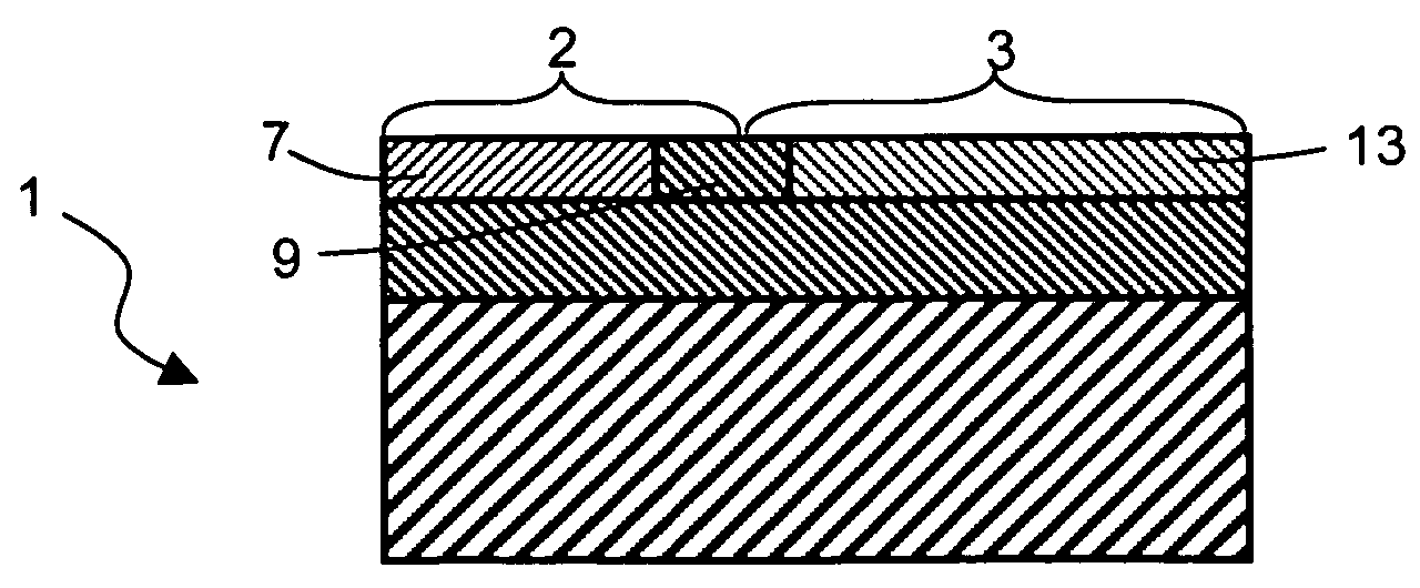
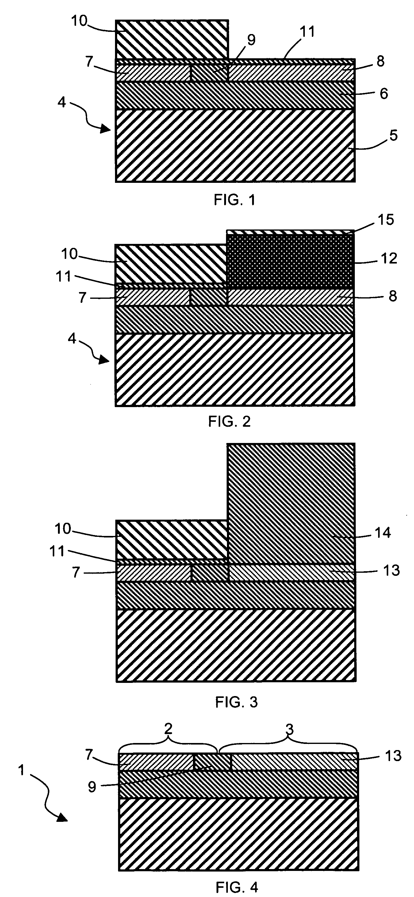
[0025]With reference to FIGS. 1 to 6, the fabrication method according to the invention is designed in particular to achieve a mixed substrate 1, i.e. presenting at least one tensile strained silicon-on-insulator (sSOI) portion 2, co-integrated with at least one compressive strained germanium-on-insulator (sGeOI) portion 3 (FIG. 4). Such a substrate 1 is more particularly designed for producing CMOS (Complementary Metal Oxide Semiconductor) circuits, tensile strained silicon-on-insulator portion 2 being designed for producing components, for example a transistor, of N-MOS type and compressive strained germanium-on-insulator portion 3 being designed for producing components, for example a transistor, of P-MOS type.

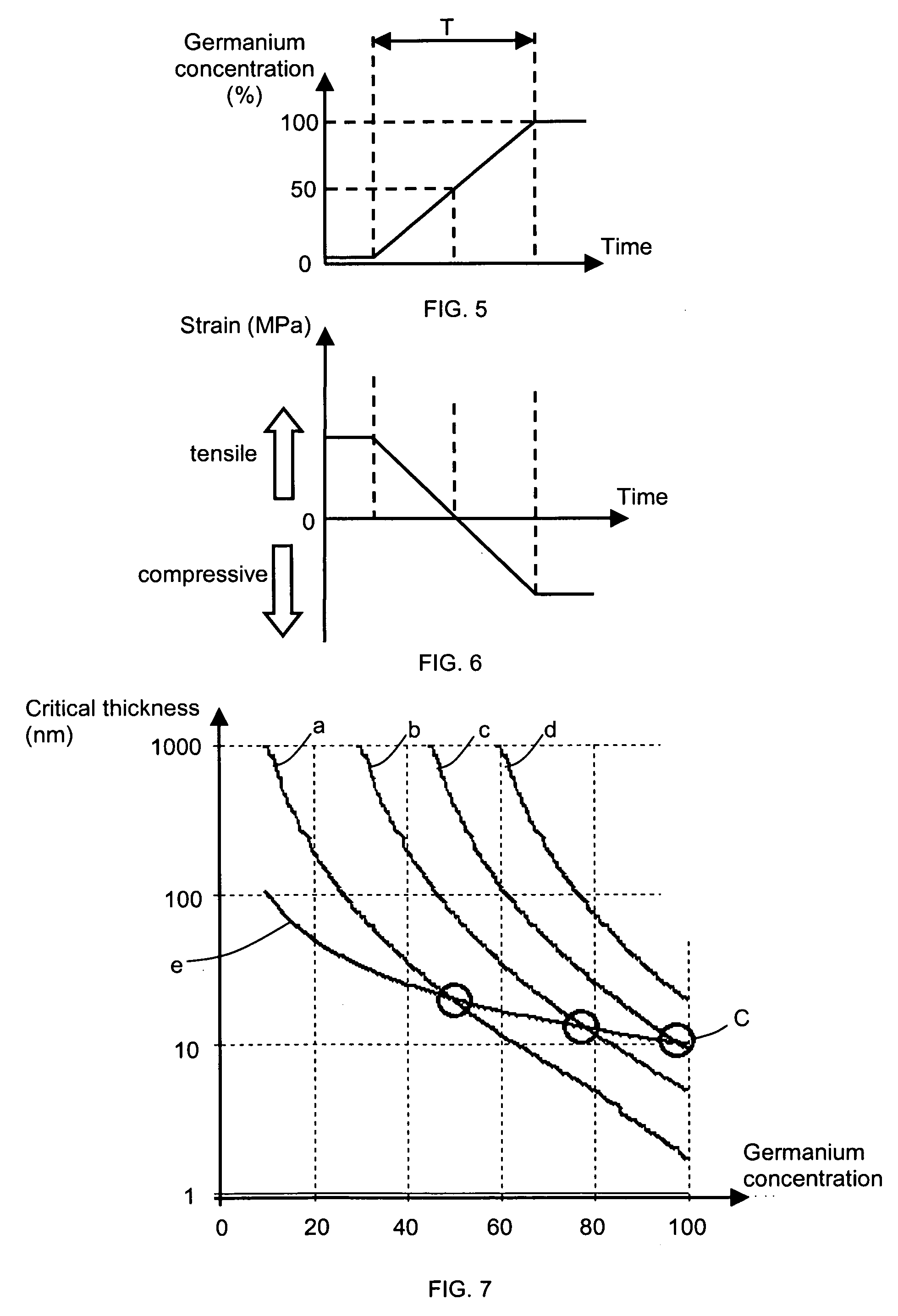
[0026]In FIGS. 1 to 4, the fabrication method consists more particularly in using a localized germanium enrichment technique, preferably by localized thermal oxidation treatment, applied on a strained silicon-on-insulator sSOI substrate. In FIG. 1, the first step of the met...


PUM

PropertyMeasurementUnit
thicknessaaaaaaaaaa
thicknessaaaaaaaaaa
tensileaaaaaaaaaa

Abstract

The fabrication method of a mixed substrate comprising a tensile strained silicon-on-insulator portion and a compressive strained germanium-on-insulator portion comprises a first step of producing a strained silicon-on-insulator base substrate comprising first and second tensile strained silicon zones. After the base substrate has been produced, the method comprises the successive steps of masking the first tensile strained silicon zone forming the tensile strained silicon-on-insulator portion of the substrate, of performing germanium enrichment treatment of the second tensile strained silicon zone of the base substrate until a compressive strained germanium layer is obtained forming said compressive strained germanium-on-insulator portion of the substrate, and of removing the masking.

Description

BACKGROUND OF THE INVENTION[0001]The invention relates to a fabrication method of a mixed substrate comprising at least one tensile strained silicon-on-insulator portion and at least one compressive strained germanium-on-insulator portion.[0002]The invention also relates to use of a substrate obtained by one such fabrication method for producing CMOS circuits comprising at least one N-MOS component produced on the tensile strained silicon-on-insulator portion of substrate and at least one P-MOS component produced on the compressive strained germanium-on-insulator portion of substrate.STATE OF THE ART[0003]The race for performance (current level, speed, etc.) in silicon-based microelectronics is in particular pushing for increasing miniaturization of the size of transistors. In parallel with this miniaturization phenomenon, approaches have been proposed for introducing new materials, in particular high-mobility materials such as germanium, and for introducing mechanical strains, a te...

Claims


Application Information

Patent Timeline
Patent Type & Authority Applications(United States)
IPC IPC(8): H01L21/321
CPCH01L21/02381H01L21/02488H01L21/02532H01L29/1054H01L21/823807H01L21/823878H01L21/84H01L21/02694
Inventor CLAVELIER, LAURENTLE ROYER, CYRILLEDAMLENCOURT, JEAN-FRANCOIS
Owner COMMISSARIAT A LENERGIE ATOMIQUE ET AUX ENERGIES ALTERNATIVES
Why Eureka
Try Eureka