Capacitor embedded printed circuit board

a printed circuit board and capacitor technology, applied in the direction of printed capacitor incorporation, printed circuit non-printed electric component association, printed capacitor incorporation, etc., can solve the problems of reduced area for mounting passive elements on a pcb, too small capacitance value to be used, etc., to achieve high capacitance per unit area and reduce high inductance

Inactive Publication Date: 2008-09-18
SAMSUNG ELECTRO MECHANICS CO LTD
View PDF7 Cites 57 Cited by
  • Summary
  • Abstract
  • Description
  • Claims
  • Application Information

AI Technical Summary

Benefits of technology

[0014]An aspect of the present invention provides a capacitor embedded printed circuit board (PCB) capable of having a higher capacitance per unit area than a convention

Problems solved by technology

However, as electronic devices become miniaturized and complicated, an area for mounting passive elements on a PCB is reduced.
Thereupon, parasitic impedances occurring due to various causes such as a conductor or solder between passive

Method used


Image

  • Capacitor embedded printed circuit board
  • Capacitor embedded printed circuit board
  • Capacitor embedded printed circuit board

Examples


Embodiment Construction

[0028]Exemplary embodiments of the present invention will now be described in detail with reference to the accompanying drawings.

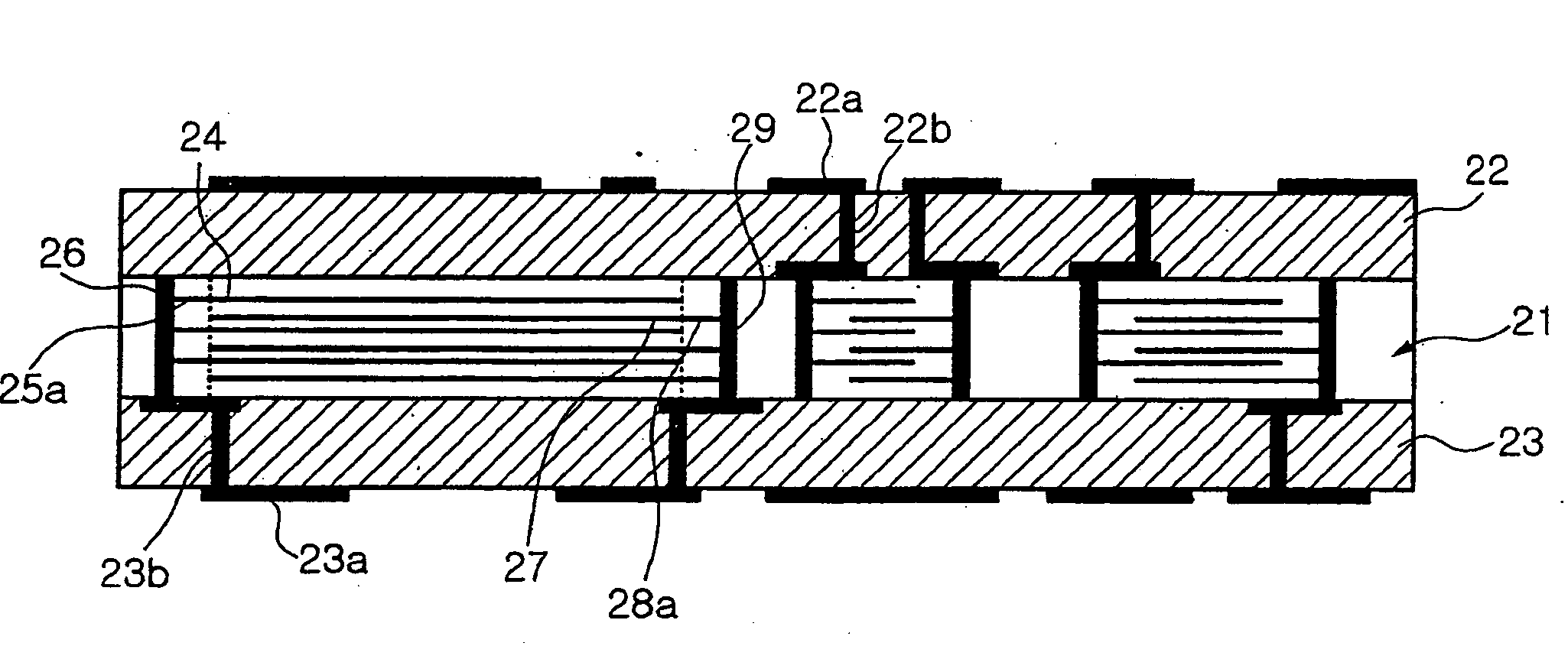
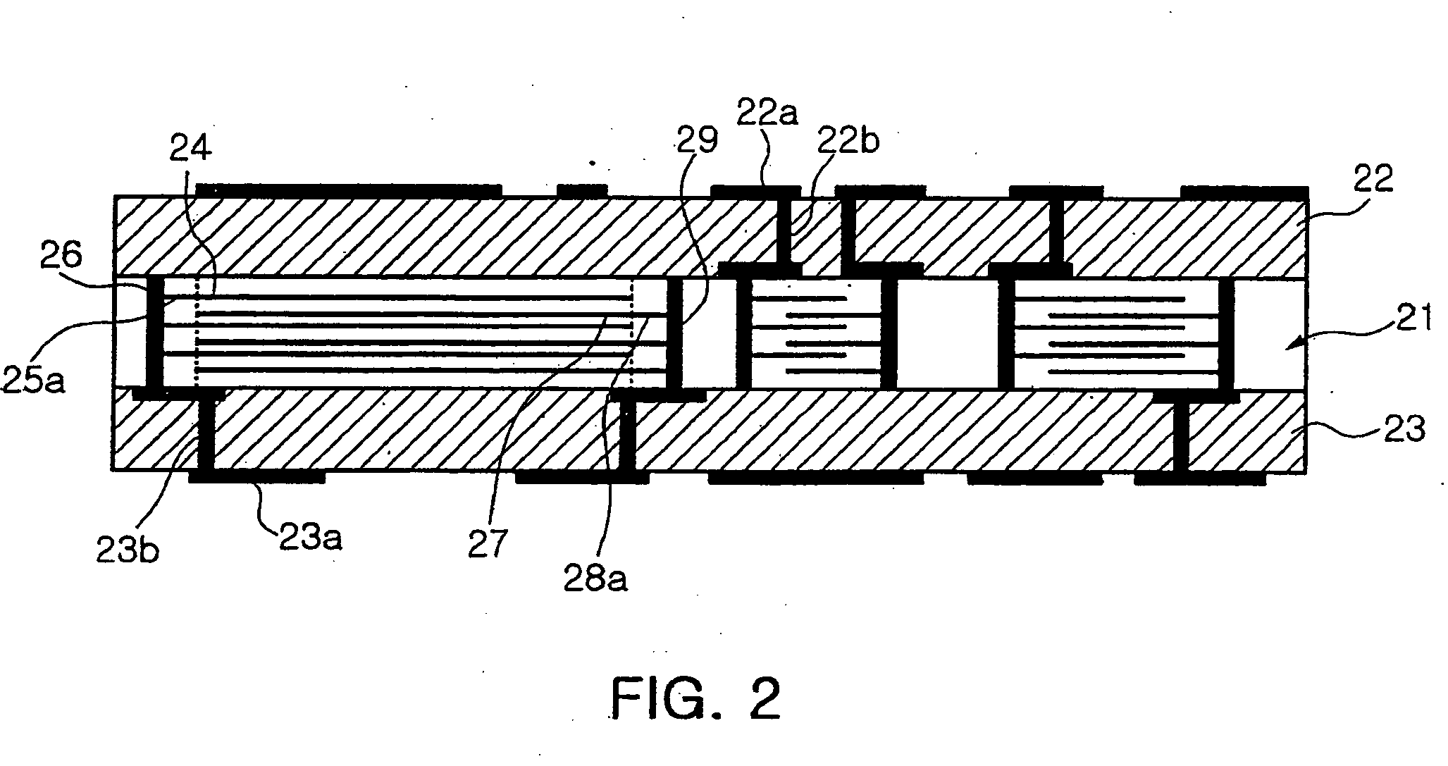
[0029]FIG. 2 is a cross-sectional view illustrating a capacitor embedded printed circuit board (PCB) according to an embodiment of the present invention.

[0030]Referring to FIG. 2, the PCB includes a multilayer polymer capacitor layer 21 where inner electrodes are formed and insulating layers 22 and 23.

[0031]The multilayer polymer capacitor layer 21 is formed of a plurality of laminated polymer sheets, and the multilayer polymer capacitor layer 21 is formed by laminating one or more of the plurality of polymer sheets where a first inner electrode 24 of conductivity is patterned on one surface thereof and a second inner electrode 27 forming a pair together with the first inner electrode is patterned.

[0032]The first inner electrode 24 is connected to a first via hole 26 for capacitor via a first extended electrode 25a, and the second inner electrode 27 is con...


PUM


Abstract

A capacitor embedded printed circuit board (PCB), the PCB including: a multilayer polymer capacitor layer where a plurality of polymer sheets is laminated; one or more first inner electrodes and second inner electrodes, separated by one or more of the plurality of polymer sheets and alternately disposed to form a pair; a plurality of first extended electrodes and second extended electrodes connected to the first inner electrodes and second inner electrodes, respectively; one or more insulating layers laminated on one or both surfaces of the multilayer polymer capacitor, where a plurality of conductive patterns and conductive via holes, forming an interlayer circuit are formed; a plurality of first via holes for capacitor, penetrating the multilayer polymer capacitor layer to be connected to the first extended electrodes; and a plurality of second via holes for capacitor, penetrating the multilayer polymer capacitor layer to be connected to the second extended electrodes, wherein the plurality of the first and second extended electrodes are alternately disposed to be opposite to each other.

Description

CROSS-REFERENCE TO RELATED APPLICATIONS[0001]This application claims the priority of Korean Patent Application No. 2007-0024071 filed on Mar. 12, 2007, in the Korean Intellectual Property Office, the disclosure of which is incorporated herein by reference.BACKGROUND OF THE INVENTION[0002]1. Field of the Invention[0003]The present invention relates to a capacitor embedded printed circuit board (PCB), and more particularly, to a capacitor embedded PCB, capable of decreasing an inductance by controlling an electrode structure of the embedded capacitor and of easily embodying high capacitance for unit area by controlling a number of multilayers and an area of electrodes.[0004]2. Description of the Related Art[0005]In general, a capacitor is a device storing energy as the form of charges and has properties, in which charges are stored and a current does not flows in the case of a direct current (DC) power source and a current flows in proportion to a change in voltage according to a capa...

Claims


Application Information

Patent Timeline
IPC IPC(8): H05K1/16
CPCH05K1/162H05K3/4602H05K2203/061H05K3/4688H05K2201/09672H05K3/4652H05K1/18
Inventor KIM, JIN CHEOLKIM, TAE KYOUNGOH, JUN ROK
Owner SAMSUNG ELECTRO MECHANICS CO LTD
Why Eureka
Try Eureka