

Methods for nanowire alignment and deposition
- Summary
- Abstract
- Description
- Claims
- Application Information
AI Technical Summary
Benefits of technology
Problems solved by technology
Method used
Image

Examples
example 1
Positioning of Nanowires
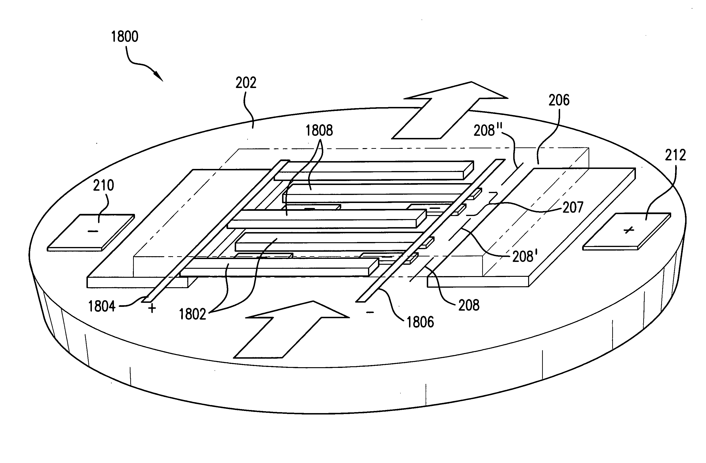
[0222]As represented in FIGS. 2 and 14a, flow channel 206 is initially filled with solvent (IPA) 1402 and subsequently with nanowire (NW) ink 1404 of a desired concentration. After introduction of a uniform film of NW ink over the wafer surface 202 the electric field is applied to the electrode (204, 205, 207) pattern. E-field parameters were about f=500 Hz and V=1 Vpp. The NWs subject to these conditions are observed to be captured / associated from suspension onto the electrodes with their long axis parallel to the electric field direction. The association can occur with the NWs pre-aligned in a fluid flow or pulled non-aligned from a stationary suspension. The NWs are observed to align adjacent to each other and exhibit a mobility along the electrode bars. This state of NW capture is referred to as weak NW “pinning” or association 1406 and is illustrated in FIGS. 5 and 8a. The mobility can be used to achieve a uniform high packing density of NWs per unit ele...
example 2
Nanowire Coupling with CNOS Nanowires
[0223]Nanowires comprising a CNOS composition (Si core), with a TaAlN outermost shell, were prepared utilizing standard growth an harvesting techniques (see e.g., Gudiksen et al (2000) “Diameter-selective synthesis of semiconductor nanowires” J. Am. Chem. Soc. 122, 8801-8802; Cui et al. (2001), “Diameter-controlled synthesis of single-crystal silicon nanowires” Appl. Phys. Lett. 78, 2214-2216; Gudiksen et al. (2001), and “Synthetic control of the diameter and length of single crystal semiconductor nanowires” J. Phys. Chem. B 105, 4062-4064). Nanowires were about 22 microns in length and about 100 nm in diameter. Suspensions of nanowires at both moderate density and low density (10-fold dilution of moderate density suspension) were prepared in isopropanol (IPA).
[0224]A 500 micron thick, 4 inch diameter quartz substrate was patterned with a plurality of Moly (Mo) electrodes, each of which was approximately 400 Å thick, and about 15 microns or about...
example 3
Nanowire Coupling on 10×10 Array
[0228]Nanowires comprising a CNOS composition (Si core), with a TaAlN outermost shell, were prepared utilizing standard growth an harvesting techniques (see e.g., Gudiksen et al (2000) “Diameter-selective synthesis of semiconductor nanowires” J. Am. Chem. Soc. 122, 8801-8802; Cui et al. (2001), “Diameter-controlled synthesis of single-crystal silicon nanowires” Appl. Phys. Lett. 78, 2214-2216; Gudiksen et al. (2001), and “Synthetic control of the diameter and length of single crystal semiconductor nanowires” J. Phys. Chem. B 105, 4062-4064). Nanowires were about 22 microns in length and about 100 nm in diameter. Suspensions of nanowires at both moderate density and low density (10-fold dilution of moderate density suspension) were prepared in isopropanol (IPA).
[0229]A 500 micron thick, 4 inch diameter quartz substrate was patterned with a 10×10 array of Moly (Mo) electrode pairs (i.e., 100 total electrode pairs, 200 total electrodes), each of which wa...
PUM
 Abstract
Description
Claims
Application Information