Pixel structure of a thin film transistor liquid crystal display

a thin film transistor and liquid crystal display technology, applied in the field of liquid crystal display, can solve the problems of increasing the power loss of the panel module, and the design cannot meet the market requirements for a higher resolution of the display panel, so as to improve the aperture ratio of pixels, reduce power loss, and improve pixel quality

Inactive Publication Date: 2008-09-18
WINTEK CORP
View PDF3 Cites 8 Cited by
  • Summary
  • Abstract
  • Description
  • Claims
  • Application Information

AI Technical Summary

Benefits of technology

[0008]The primary objective of the present invention is to overcome the shortcomings of the prior art by increasing the aperture ratio of pixels regardless of being applied to a high-resolution panel or a low-resolution panel, so as to improve the pixel quality and correspondingly reduce the power loss caused by improving the brightness of a backlight module.
[0009]To achieve the foregoing objective, a pixel structure of a thin film transistor liquid crystal display in accordance with the present invention comprises a substrate, a first metal conductive layer covered onto the substrate, a first insulating layer (a gate insulating layer), a hydrogenated amorphous silicon (a-Si:H) intrinsic layer and an n+Si ohmic contact film coated onto the first metal conductive layer, a second metal conductive layer and a second insulating layer coated onto the second metal conductive layer, an organic insulating layer covered onto the second insulating layer, a third metal conductive layer covered onto the organic insulating layer, a passivation layer covered onto the third metal conductive layer, and a transparent conductive layer covered onto the passivation layer, characterized in that the organic insulating layer having a low dielectric constant lowers the parasitic capacitance produced by the data signal line of the second metal conductive layer and the common electrode (Vcom) of the third metal conductive layer, while the pixel electrode comprised of the common electrode and the transparent conductive layer and including a passivation layer acts as a storage capacitor required for the pixels, and the opaque characteristic of the common electrode (Vcom) can prevent light leaks and shield extra light of the backlight module in the LCD, such that the light sources between pixels will not interfere with each other, so as to enhance the display contrast.

Problems solved by technology

Since such brightness is insufficient, an increase of the brightness of the backlight module can increase the brightness of the pane, which will also increase the power loss of the panel module.
Such design cannot comply with the market requirements for a higher resolution of the display panel (or a smaller pixel size).

Method used


Image

  • Pixel structure of a thin film transistor liquid crystal display
  • Pixel structure of a thin film transistor liquid crystal display
  • Pixel structure of a thin film transistor liquid crystal display

Examples


Embodiment Construction

[0030]The technical characteristics, features and advantages of the present invention will become apparent in the following detailed description of the preferred embodiments with reference to the accompanying drawings.

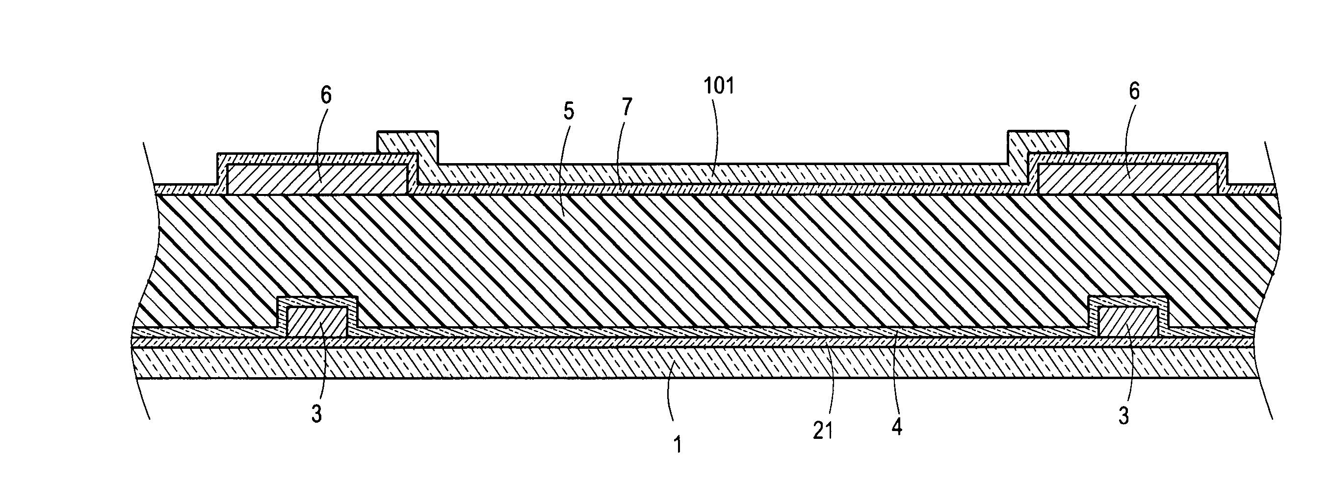
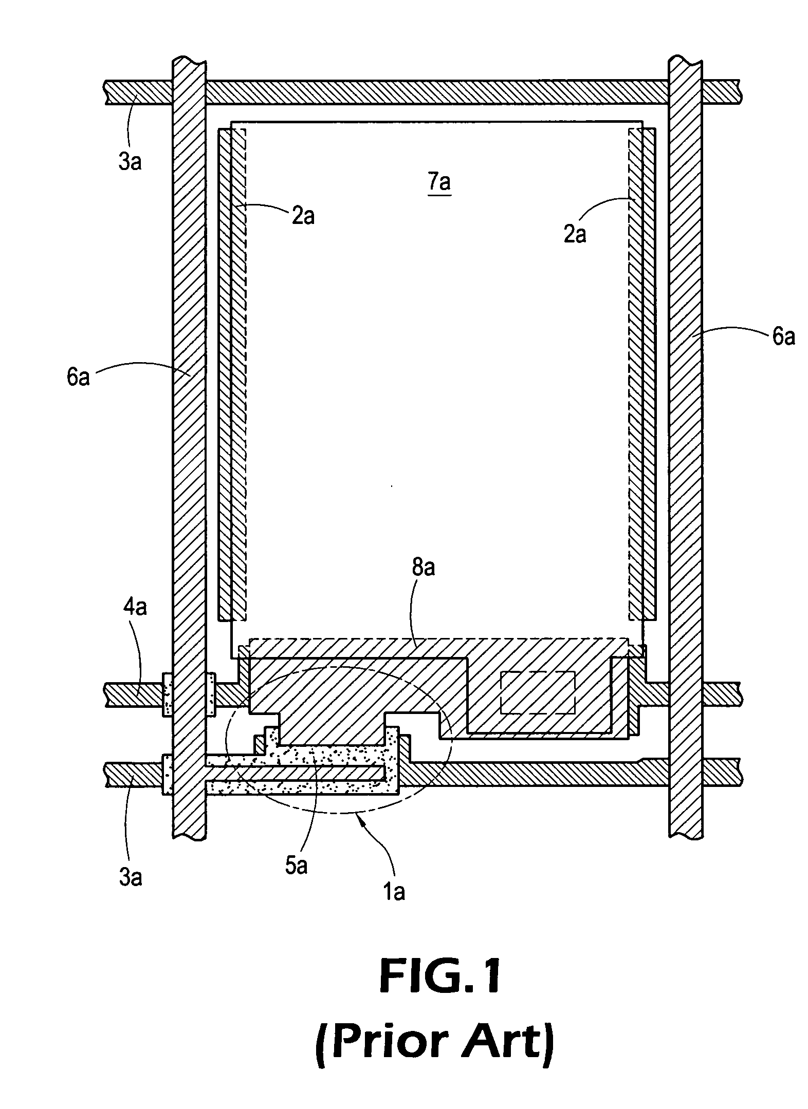
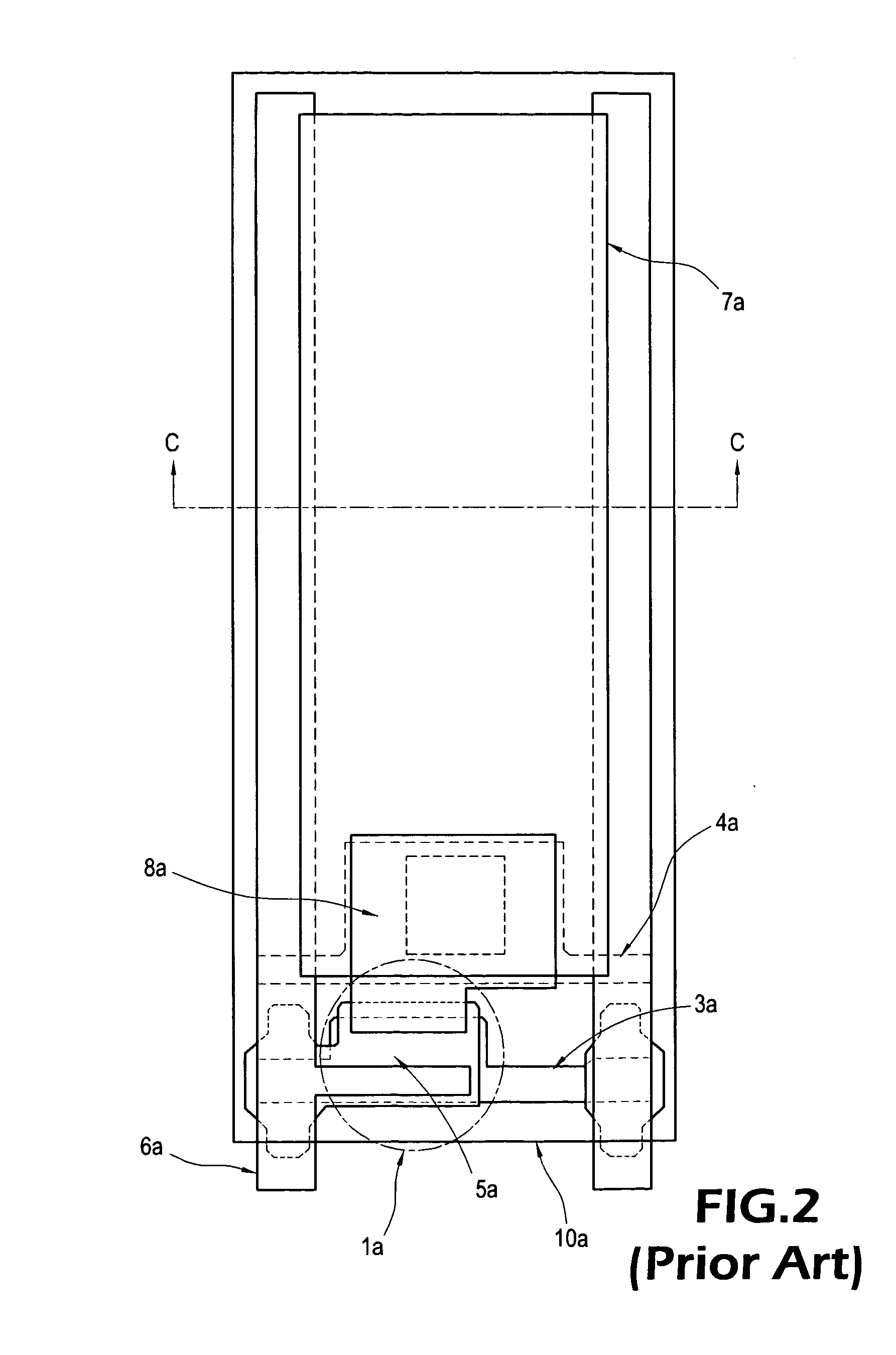
[0031]Referring to FIGS. 4 to 19 for the manufacturing flow of a pixel structure of a liquid crystal display according to a preferred embodiment of the present invention, the pixel structure of a thin film transistor liquid crystal display of the invention increases the pixel aperture ratio to improve the brightness and the display quality of the display panel and enhance product competitiveness.

[0032]The pixel structure of a thin film transistor liquid crystal display in accordance with the invention comprises: a TFT structure 9, a scan signal line 11 formed by a first metal conductive layer, an active region 10, a data signal line 3 formed by a second metal conductive layer, a common electrode 6 of a third conductive layer, a pixel electrode 101 of a transparent cond...


PUM


Abstract

A pixel structure of a thin film transistor liquid crystal display employs a design of three metal layers and includes an organic insulating layer between a data signal line and a common electrode for reducing a parasitic capacitance, while a passivation layer included between the common electrode and a pixel electrode acts as a storage capacitor required for the pixels, so as to achieve a high aperture ratio, and the common electrode can act as a shielding bar for enhancing the display contrast.

Description

BACKGROUND OF THE INVENTION[0001]1. Field of the Invention[0002]The present invention relates to a liquid crystal display, and more particularly to a pixel structure of a thin film transistor liquid crystal display.[0003]2. Description of Prior Art[0004]Liquid crystal display (LCD) becomes increasingly popular due to its low radiation and compact size, and thin film transistor LCD (TFT LCD) is a mainstream display product in the market due to its contrast and viewing angle.[0005]Since liquid crystals are non-luminous materials, the light source of the TFT LCD is a backlight light source, and the backlight light source can pass through the materials of each layer of the TFT LCD such as a polarizer and a color filter to provide a display brightness approximately equal to 10% of the brightness of the original light source. Since such brightness is insufficient, an increase of the brightness of the backlight module can increase the brightness of the pane, which will also increase the po...

Claims


Application Information

Patent Timeline
Patent Type & Authority Applications(United States)
IPC IPC(8): H01L21/336
CPCG02F1/1362H01L27/1255G02F2201/40G02F1/136213
Inventor TSAI, CHE-FUCHOU, YI-LINWANG, WEN-CHUN
Owner WINTEK CORP
Why Eureka
Try Eureka