[0015]It is therefore an object of the present invention to provide a method of producing a wafer scale package of at least two wafers that enables a precise control of the position of an optical element that is produced by means of a replication technique on a first wafer with respect to a functional element or another reference on a second wafer, e.g. the front or back surface of the second wafer. In particular, it is desirable to control said position as measured in a direction perpendicular to the wafer plane.
[0030]The following effect is achieved by the invention: The front surface of the first substrate defines an
abutment /
reference plane of the first substrate serving as a stop for the replication tool. This plane, thus, confines movement of the replication tool towards the first substrate. Because the replication tool abuts at the
abutment plane of the first substrate, the
abutment plane acts as a reference such that the
axial distance between this reference and the replicated optical element (more particularly, a given
surface point thereof, e.g. the vertex of a lens) is fixed. This axial distance corresponds to the axial distance of the replication sections to a tool
reference plane that is, for example, defined by those surface structures of the tool that abut at the first substrate. It can thus be precisely controlled by choosing an appropriate shape of the tool. This has the
advantage that the exact amount of replication material does not influence the axial position of the optical element with respect to the first surface
reference plane. In particular if the first substrate comprises the at least one recess, the shape of this recess itself does not influence the axial position of the optical element. Variations of the
surface structure of the first substrate are compensated by the replication material. Furthermore, the abutment plane also serves for correct positioning of the second substrate. Generally, a front or back surface of the second substrate may be considered as defining a second substrate abutment plane, and the two abutment planes are brought in overlapping relationship. Consequently, the distance of the optical element with respect to the second substrate or any further element arranged at the second substrate in a given
spatial relationship to the second substrate abutment plane, e.g. at a front or back surface of the second substrate, is well defined.
[0033]Preferably, a
maximum depth of the at least one recess is greater than a maximum height of the replication sections with respect to the tool reference plane. If the recess is in the second substrate, a planar unstructured first substrate can be used, and vice versa. This simplifies manufacture of the wafer package.
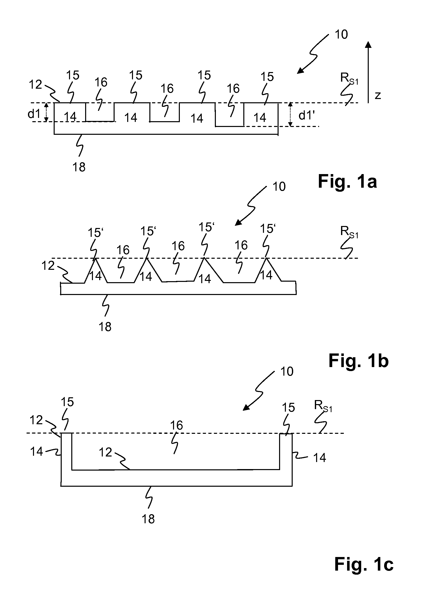
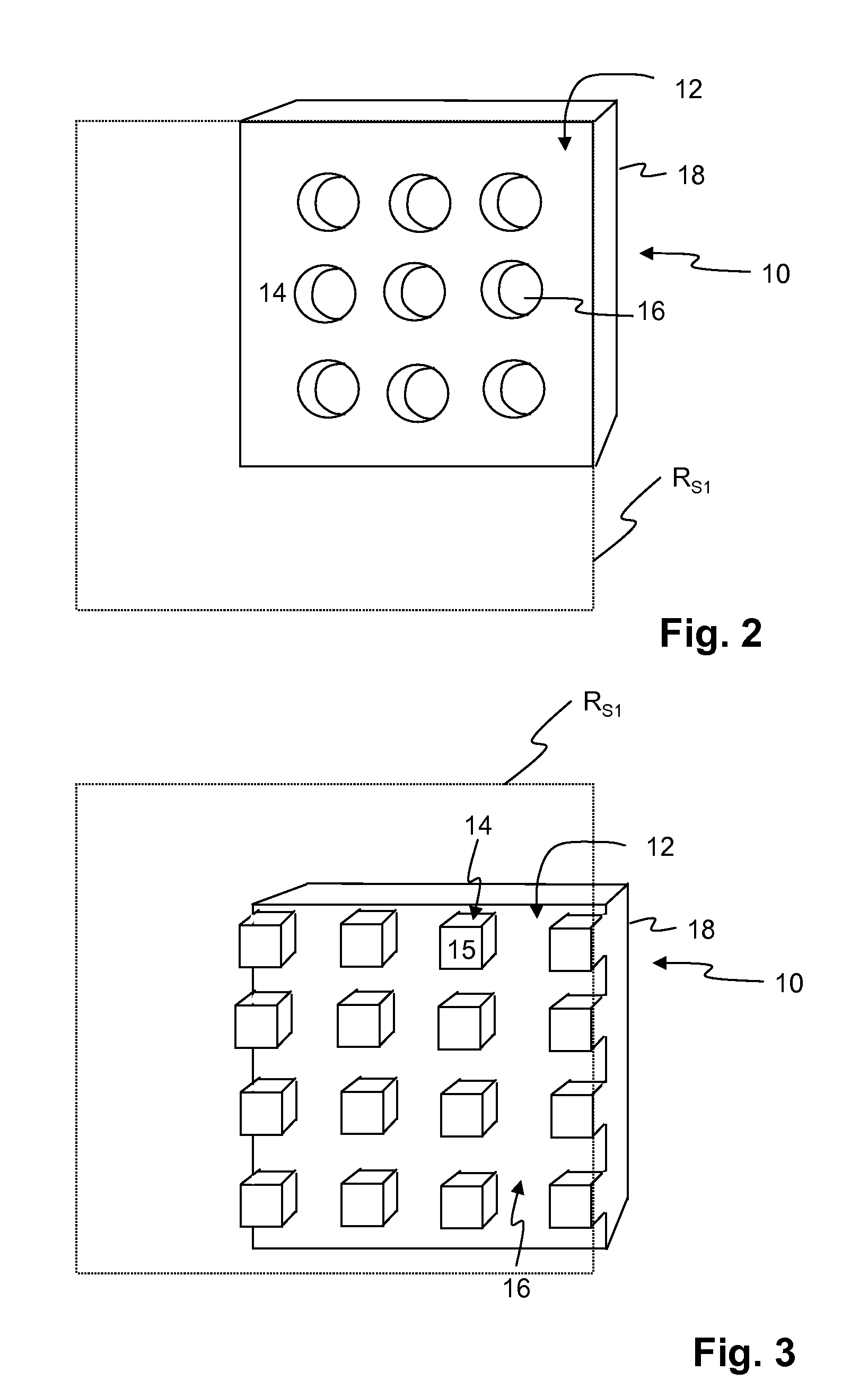
[0039]Generally, the front surface of the pre-shaped substrate may have any shape or structure that is sufficient to define an abutment plane. For example, the abutment plane may only be defined by a plurality of spikes protruding from an otherwise flat front surface or a continuous rim arranged at the perimeter of the wafer, and the major part of the front surface may be considered as a “recess”. However, the following preferred embodiments have advantages concerning the production of the wafer, the stability during manufacture of the wafer package and the precision of positioning the optical elements.
[0040]In such a preferred embodiment of the invention, the pre-shaped substrate comprises a plurality of recesses formed in an otherwise planar front surface. The recesses may, for example, have a cylindrical shape, preferably with a circular cross section. Each of the recesses is, for example, intended to receive only one optical element. In this case, a portion of the replication material applied directly to a recess is confined by lateral walls of the recess. Another preferred embodiment comprises a plurality of protrusions having a planar front face, arranged on an otherwise flat front surface (the recess then corresponds to those parts of the front surface that are not protrusions). Both arrangements are very stable with respect to bending or flexing as the other substrate and in some embodiments also the replication tool abut at and are supported by a significant part of the front surface of the pre-shaped substrate. This simplifies manufacture of the wafer package.
[0043]The pre-shaped substrates used in the inventive method are generally made of a single piece. They can be manufactured by known methods, e.g. by
etching. In this example, the abutment plane may correspond to those parts of the originally planar front surface of the substrate that are not etched away. As discussed above, the invention has the
advantage that tolerances in the dimensions of the pre-shaped wafer can be compensated by the
replication process.

