

Ramp generator and circuit pattern inspection apparatus using the same ramp generator
a technology of circuit pattern inspection and ramp generator, which is applied in the direction of pulse technique, basic electric elements, electric discharge tubes, etc., can solve the problem of difficult offset control of deflection that is necessary in an apparatus
- Summary
- Abstract
- Description
- Claims
- Application Information
AI Technical Summary
Benefits of technology
Problems solved by technology
Method used
Image

Examples
first embodiment
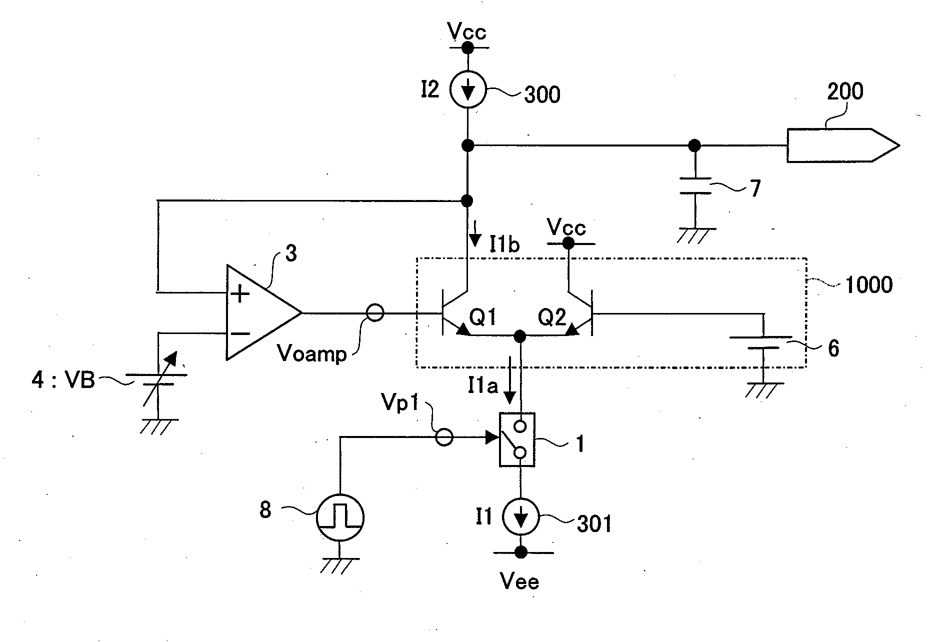
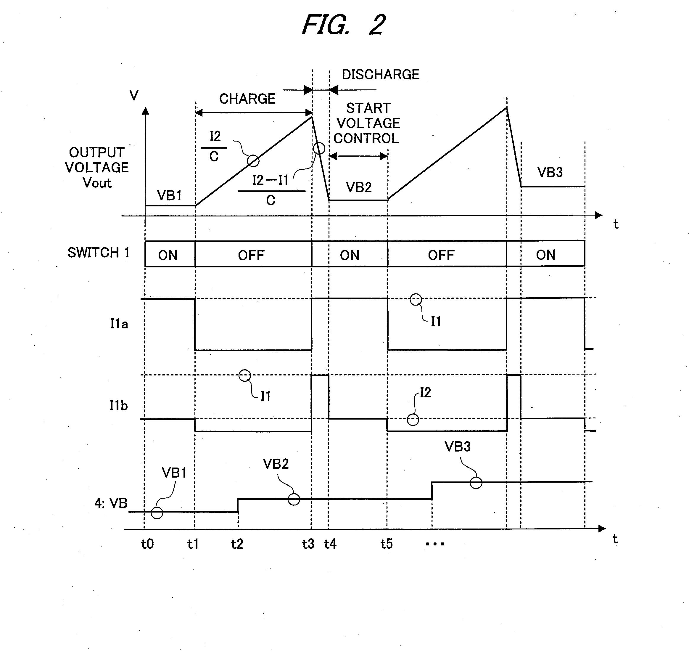
[0032]FIG. 1 is a circuit diagram showing a first embodiment of a ramp generator according to the present invention, and FIG. 2 is a waveform chart showing an operation waveform when the circuit is operated.
[0033]The ramp generator according to the present embodiment is configured of a switch 1, an amplifier 3, a variable reference voltage generation unit 4, a reference voltage generation unit 6, an integration capacitor 7, a timing signal generation unit 8, a transistor Q1, a transistor Q2, an output terminal 200, a constant current source (charge current source) 300, and a constant current source (discharge current source) 301. A current value of the charge current source 300 is defined as I2 and a current value of the discharge current source 301 is defined as I1.
[0034]The transistor Q1 and the transistor Q2 are both NPN transistors, and such two transistors constitute a differential pair. A collector terminal of the transistor Q1 is connected to Vcc via the charge current source...
second embodiment
[0050]Next, a second embodiment of the present invention will be described with reference to FIG. 3 and FIG. 4.
[0051]FIG. 3 is a circuit diagram of a ramp generator of the present embodiment, and FIG. 4 is a waveform chart showing the operation waveform when the circuit is operated. The circuit will first be described based on FIG. 3.
[0052]In the present embodiment, the switch 1, the variable reference voltage generation unit 4, the reference voltage generation unit 6, the timing signal generation unit 8, the transistor Q1, the transistor Q2, the output terminal 200, and the charge / discharge current source 300 have a configuration similar to that of the first embodiment.
[0053]On the other hand, in place of the integration capacitor 7 of the first embodiment, a current integrator 7′ including an amplifier 11 and a capacitor 12 is disposed. The capacity of the capacitor 12 is defined as C2.
[0054]Further, in place of the amplifier 3, an amplifier circuit (differential amplifier) 3′ inc...
third embodiment
[0074]Next, a third embodiment of the present invention will be described with reference to FIG. 5, FIG. 6, and FIG. 7.
[0075]In the second embodiment, the timing control at the discharge needs to be accurately performed. This problem will be described in FIG. 5.
[0076]The timing (timing to open the switch 2) of t4′ in FIG. 5 and the timing of t4 in FIG. 3 will be focused.
[0077]That is, when there is the response delay time td of the current adjustment unit 1000 from the output of the current integrator 7′ and the opening of the switch 2 is delayed at the discharge, the voltage Vout of the output terminal 200 continuously rises until td with dV / dt=((I1+I1′−I2) / C2). Then, when the time at which the current adjustment unit 1000 responds is reached (t4′ in FIG. 5), the output voltage Vout starts to decrease with dV / dt=−(I2 / C2) and finally converges to Vout=VB2.
[0078]However, if the convergence to the start voltage delays due to the difference in timing, “stability of output of start volt...
PUM
 Abstract
Description
Claims
Application Information