Light emitting device and method of producing the same

a technology of light emitting devices and light sources, which is applied in the direction of semiconductor/solid-state device manufacturing, semiconductor devices, electrical devices, etc., can solve the problems of affecting the efficiency of light emission, and the damage of the element per se, so as to improve the intensity of light emitted, improve the efficiency of light emitted, and improve the effect of long-term reliability

Inactive Publication Date: 2008-10-02
SHARP KK
View PDF7 Cites 33 Cited by
  • Summary
  • Abstract
  • Description
  • Claims
  • Application Information

AI Technical Summary

Benefits of technology

[0023]The present invention is in view of the foregoing problems, and has as an object to provide a light emitting device, and a method of producing the light emitting device, that is reduced in light leakage and improved in intensity of light emitted from a light outgoing surface and in heat releasing property to have excellent long-term reliability.
[0025]With this structure, light that is emitted from the LED chip and enters the insulating section is reflected by the light reflective filler-added area. This makes it possible to reduce light that is partially absorbed and becomes attenuated when entering the insulating section and being reflected by a peripheral component, so that efficiency for light utilization and heat releasing property improve.
[0027]With this structure, the metallic reflecting plate that reflects light emitted from the LED chip and guides the light to the light outgoing surface provided in the direction in which the light is emitted is provided, in the direction in which the LED chip emits light, in such a manner as to surround the LED chip entirely. This allows the metallic reflecting plate to reflect light emitted from the LED chip to its surroundings and guides the light to the light outgoing surface efficiently. Thus, light leaking from a side surface of the element is reduced so that the intensity of light emitted from the light outgoing surface improves. Further, the inner side surface of the metallic reflecting plate closely adheres to the light-transmitting sealant. This makes it possible to prevent a problem that the metal peels off the inner side surface of the metallic reflecting plate. Thus, the inner side surface of the metallic reflecting plate is protected stably with the light-transmitting sealant.
[0028]Further, the first metal layer functions as a mount-surface metallic reflecting film and is formed so as to surround an outer edge of the second metal layer via the insulating section formed around an outer edge of the second metal layer. This makes it possible to form the first metal layer, which serves as the mount-surface metallic reflecting film, all over an area outside of a part of the mount surface of the substrate, which part includes the insulating section, while the first metal layer is kept isolated from the second metal layer. The first metal layer serving as the mount-surface metallic reflecting film is formed over a wide area of the mount surface. This allows much of light emitted from the LED and traveling toward the substrate to be guided to the light outgoing surface efficiently by the first metal section. Thus, it becomes possible to further reduce the amount of light absorbed by the substrate, so that the intensity of light emitted from the light outgoing surface improves.
[0029]Further, the insulating section is made of resin containing the light reflective filler. This allows light emitted from the LED chip and entering the insulating section to be reflected by the light reflective filler. Thus, it becomes possible to reduce light that is partially absorbed and becomes attenuated when entering the insulating section and being reflected by a peripheral component, so that the intensity of light emitted from the light outgoing surface improves.

Problems solved by technology

Further, if heat generated in the light emitting device is not sufficiently radiated, the heat damages members of the element, so that light emission efficiency drops or the element per se is damaged.
As a result, it is impossible to keep the long-term reliability.
Thus, the light emitted from the LED chip 103 cannot be efficiently guided to the light projecting surface of the light emitting device 101 and cannot be projected outward from the element.
Further, variation in an amount of the fluorescent particles changes scattering degree, so that the light cannot be stably projected outward.
However, in a conventional structure described in Publication 1, as a distance between an upper surface of the LED chip 103 and the reflecting film 121 is shorter, the light absorption / light leakage results in greater loss.
Hence, this raises such a problem that light is much less efficiently projected outward from the light emitting device.
This results in great energy loss in all.
Thus, light emitted from the LED chip cannot be efficiently projected outward, so that intensity of light projected from the light projecting surface decreases.

Method used


Image

  • Light emitting device and method of producing the same
  • Light emitting device and method of producing the same
  • Light emitting device and method of producing the same

Examples


first embodiment

[0075]The following describes an embodiment of the present invention, with reference to FIGS. 1-5 and 38-41.

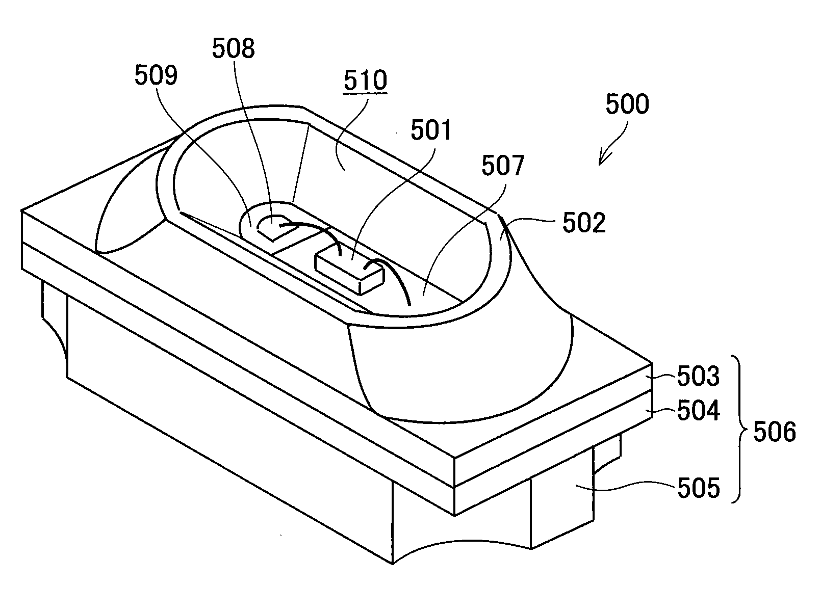
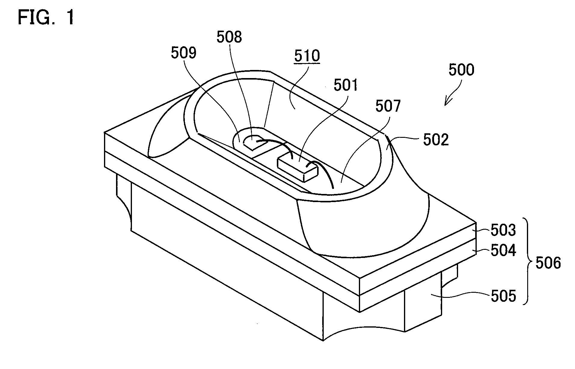
[0076]FIG. 1 is an oblique perspective view showing an exemplary structure of a light emitting device 500 of the present embodiment.

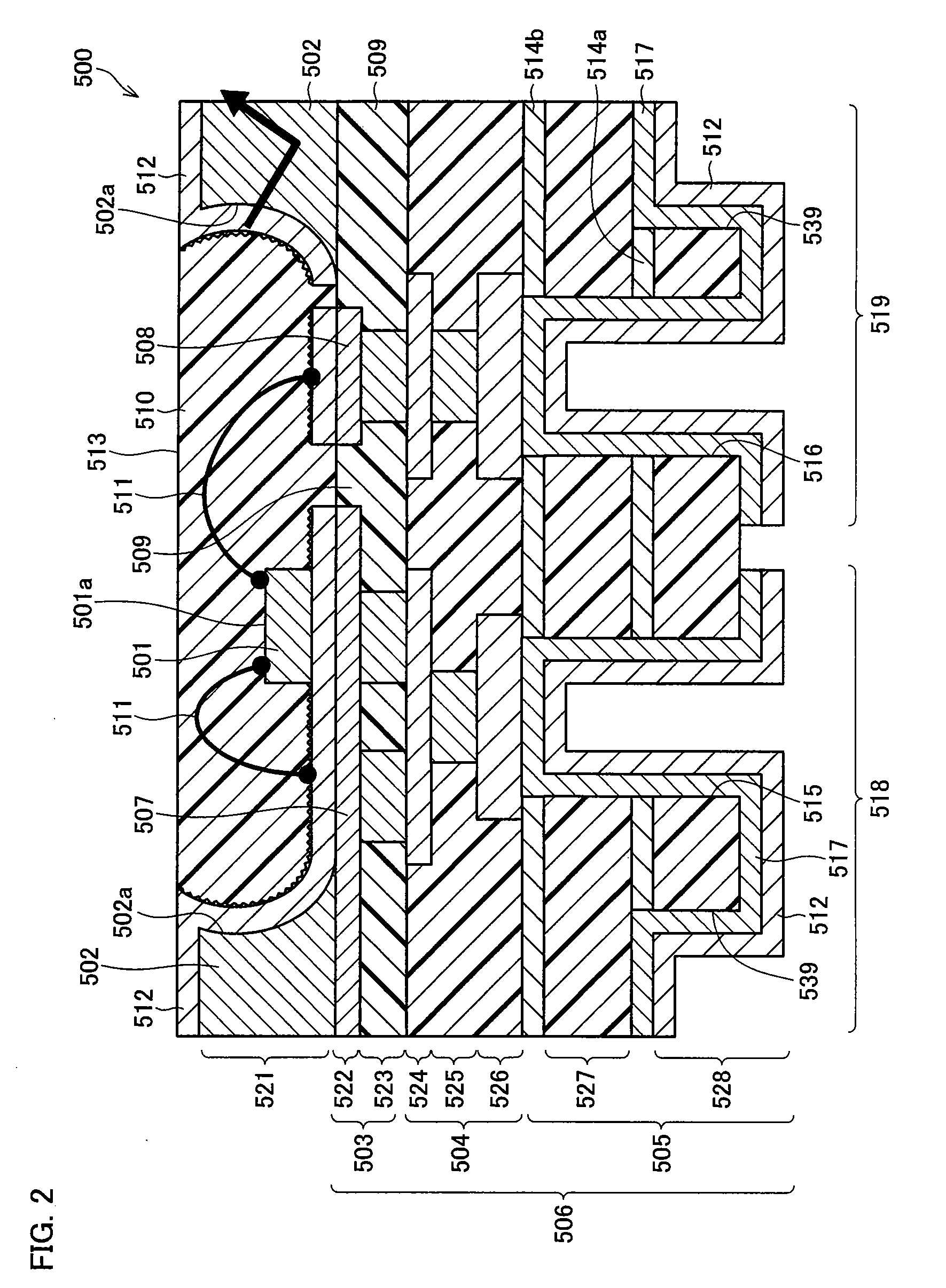
[0077]FIG. 2 is a sectional view showing a detailed structure of the light emitting device 500.

[0078]FIG. 3 shows a pattern of etching a metallic reflecting plate 502 and respective layers that constitute a multilayer substrate 506. FIG. 3(a) shows a first layer 521. FIG. 3(b) shows a second layer 522. FIG. 3(c) shows a third layer 523. FIG. 3(d) shows a fourth layer 524. FIG. 3(e) shows a fifth layer 525. FIG. 3(f) shows a sixth layer 526. FIG. 3(g) shows a seventh layer 527. FIG. 3(h) shows an eighth layer 528.

[0079]As shown in FIG. 1, the light emitting device 500 of the present embodiment includes an LED chip 501, which is mounted on the multilayer substrate 506, and the metallic reflecting plate 502. The metallic reflecting plate 502 stands a...

second embodiment

[0176]The following describes an embodiment of the present invention, with reference to FIGS. 6-14 and 23-26. For the convenience of explanation, components having the same functions as those of the components shown in the figures of the foregoing embodiments are given the same reference numbers, and description thereof is omitted.

[0177]A light emitting device 600 of the present embodiment produces an excellent effect of preventing light from leaking, in addition to the advantageous effects that the light emitting device 500 of First Embodiment produces. Further, the number of layers in a multilayer substrate 606 is reduced. The following description focuses on the structure that produces the advantageous effects and how it works to produce the advantageous effects.

[0178]In the light emitting device 500 of First Embodiment, a boundary surface between an insulating section 509 and a die-bonding-area / electrode section 507 forms a straight line when viewed from a direction vertical to ...

third embodiment

[0227]The following describes another embodiment of the present invention, with reference to FIGS. 17, 18, and 27-31. For the convenience of explanation, components having the same functions as those of the components shown in the figures of the foregoing embodiments are given the same reference numbers, and description thereof is omitted.

[0228]A light emitting device 700 according to the present embodiment includes a multilayer substrate same as the multilayer substrate 506 of the light emitting device 500 of First Embodiment discussed above.

[0229]As shown in FIG. 17, every electrode connected to an LED chip 701 and serving as an electrode terminal to supply driving current to the LED chip 701 is an island electrode. Specifically, a metallic reflecting plate 702 that reflects light from the LED chip 701 to guide the light to a light outgoing surface 513 provided in a direction in which light is emitted is electrically isolated from every electrode that supplies driving current to t...


PUM


Abstract

To provide a light emitting device that is improved in intensity of light emitted from a light outgoing surface and has excellent heat releasing property, the light emitting device according to the present invention includes an LED chip 501 mounted on a substrate and an insulating section 509 formed on a front surface of the substrate and made of light-transmitting resin. The insulating section 509 has a multilayer structure constituted of a titanium dioxide-added resin layer 509c to which titanium dioxide is added and a titanium dioxide-free resin layer 509b to which no titanium dioxide is added.

Description

[0001]This Nonprovisional application claims priority under 35 U.S.C. § 119(a) on Patent Application No. 094991 / 2007 filed in Japan on Mar. 30, 2007, and Patent Application No. 077425 / 2008 filed in Japan on Mar. 25, 2008, the entire contents of which are hereby incorporated by reference.FIELD OF THE INVENTION[0002]The present invention relates to a light emitting device that is suitable for applying light to a thin display, such as a liquid crystal panel, from a side of the display, and relates to a method of producing the light emitting device.BACKGROUND OF THE INVENTION[0003]Conventionally, as a backlight for laterally illuminating a display panel of liquid crystal or the like, a light emitting device such as a laterally light emitting diode (this diode will be referred to as “LED” hereinafter) mentioned in Japanese Unexamined Patent Publication No. 223082 / 2005 (Tokukai 2005-223082) (Publication date: Aug. 18, 2005) (this publication will be referred to as “Publication 1” hereinaf...

Claims


Application Information

Patent Timeline
Patent Type & Authority Applications(United States)
IPC IPC(8): H01L33/00H01L33/48H01L33/60H01L33/64
CPCH01L33/486H01L33/60H01L33/64H01L33/647H01L2224/48091H01L2224/48227H01L2224/48237H01L2924/00014H01L2224/48137H01L2224/49113
Inventor TAKEMOTO, MASASHI
Owner SHARP KK
Why Eureka
Try Eureka