Nonvolatile semiconductor memory system

a nonvolatile, memory system technology, applied in semiconductor devices, digital storage, instruments, etc., can solve problems such as data erroneously programmed, memory cell size, and reducing the reliability of nand-type flash memory

Inactive Publication Date: 2008-10-02
KK TOSHIBA
View PDF6 Cites 165 Cited by
  • Summary
  • Abstract
  • Description
  • Claims
  • Application Information

AI Technical Summary

Problems solved by technology

However, with the subdivision of the threshold voltage and with the decrease in the size of the memory cell, data is erroneously programmed, particularly, to the memory cell transistors adjacent to the select gate transistor.
Thus, there was a problem that the reliability of the NAND-type flash memory decreases.
To solve such a problem, a method has been proposed in which a dummy cell transistor that is not used to store data is provided next to the select gate transistor, which, however, was insufficient to prevent the decrease of reliability (see JP-A-2006-186359, for example).

Method used


Image

  • Nonvolatile semiconductor memory system
  • Nonvolatile semiconductor memory system
  • Nonvolatile semiconductor memory system

Examples


first embodiment

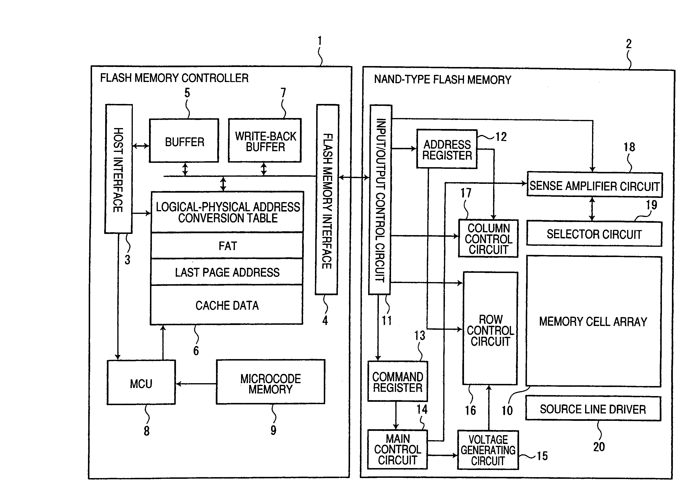
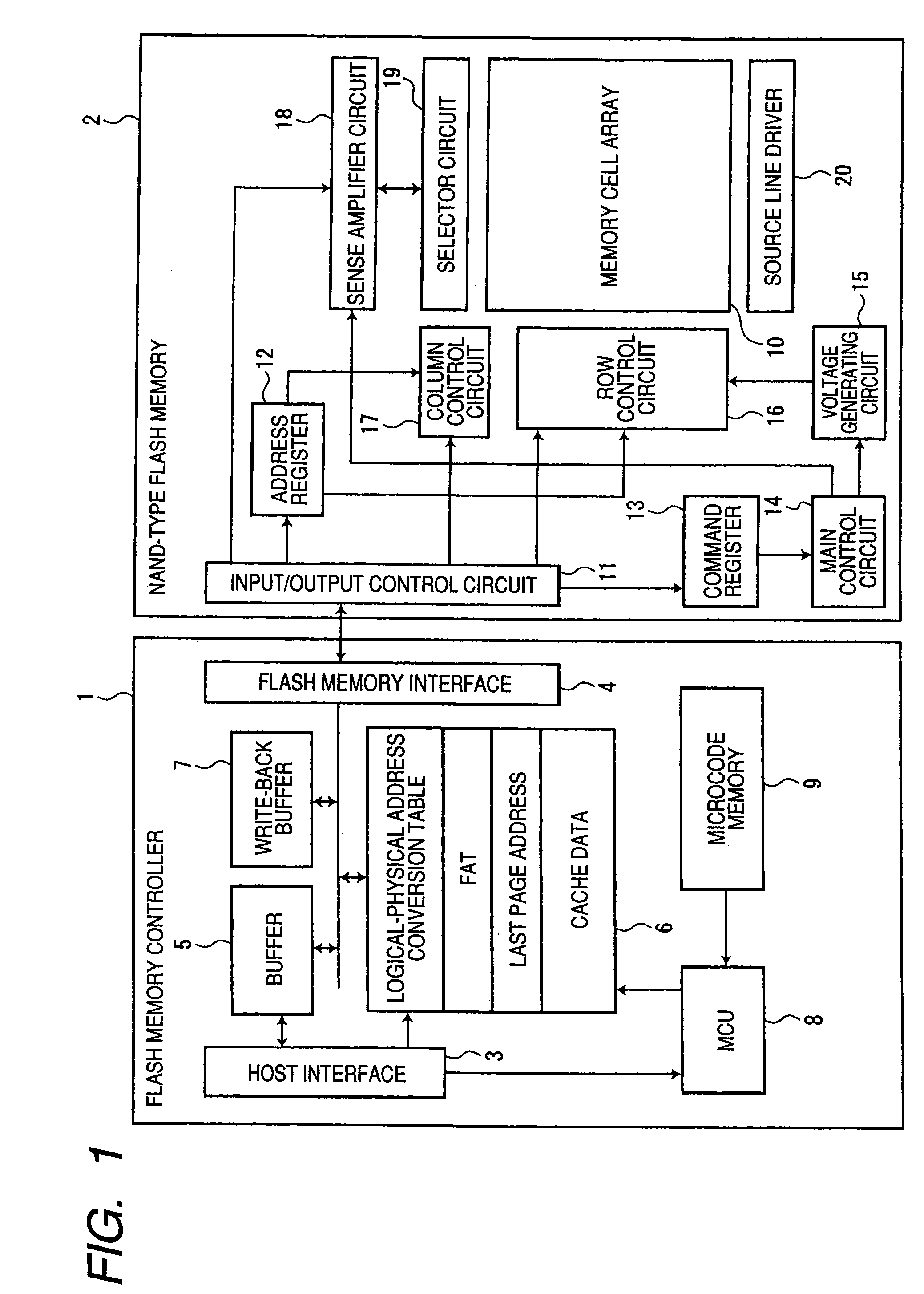
[0040]FIG. 1 is a block diagram showing the arrangement of a nonvolatile semiconductor memory system according to a first embodiment of the invention.

[0041]The memory system according to the present embodiment includes a flash memory controller (hereinafter referred to as a memory controller) 1 and a nonvolatile semiconductor memory, for example, a NAND-type flash memory 2, that is controlled by the memory controller 1.

[0042]The memory controller 1 includes a host interface 3, a flash memory interface 4, a buffer 5, a ferroelectric memory (hereinafter referred to as FeRAM (Ferroelectric Random Access Memory)) 6 as a storage portion, a write-back buffer 7, an MCU (Micro Control Unit) 8, and a microcode memory 9.

[0043]The host interface 3 interfaces between a host device (not shown) and the memory controller 1, and the flash memory interface 4 interfaces between the memory controller 1 and the NAND-type flash memory 2. Here, the host device means various electronic devices that contro...

second embodiment

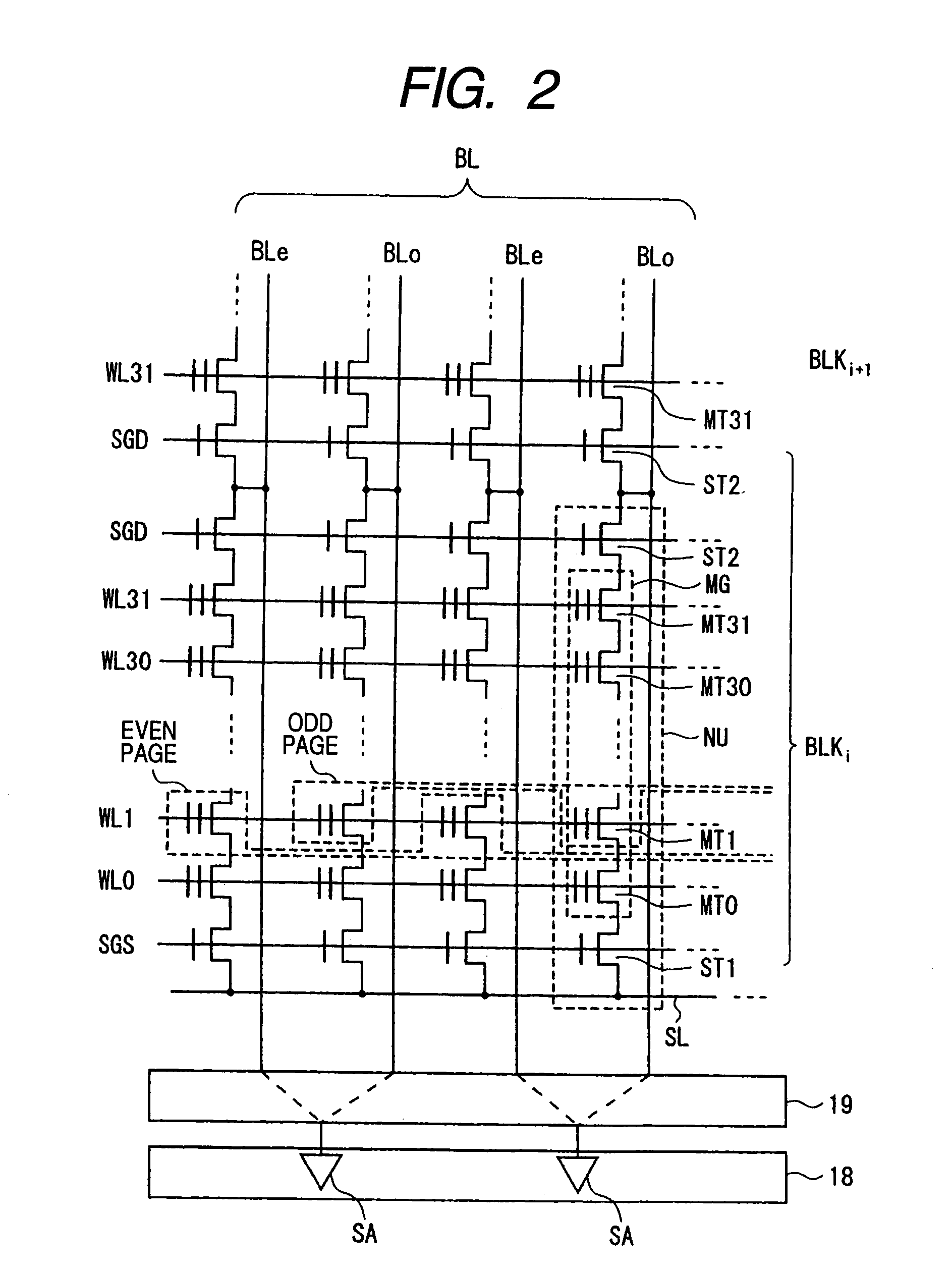
[0182]A data program operation of a memory system according to a second embodiment of the invention will be described with reference to FIG. 16. FIG. 16 is a schematic diagram showing a lower page program operation and an upper page program operation for the memory cell transistor MT0 connected to word line WL0 or the memory cell transistor MT31 connected to word line WL31 in the memory system according to the present embodiment. Hereinafter, components substantially the same as those of the first embodiment will be denoted by the same reference numerals, and only characterizing portions of the present embodiment will be described.

[0183]The memory system of the present embodiment is different from that of the first embodiment in that during data program operations for the memory cell transistor MT0 connected to word line WL0 or the memory cell transistor MT31 connected to word line WL31, a verify voltage that defines the threshold voltage lower limit of each data is set lower by VD,...

third embodiment

[0191]A data program operation of a memory system according to a third embodiment of the invention will be described with reference to FIG. 18. FIG. 18 is a schematic diagram showing the data program operation of the memory system according to the present embodiment. Hereinafter, components substantially the same as those of the first embodiment will be denoted by the same reference numerals, and only characterizing portions of the present embodiment will be described. The memory system according to the present embodiment is different from that of the first embodiment in that the memory cell transistor MT stores 16-value data depending on a threshold voltage.

[0192]Each of the memory cell transistors MT can store one of 16-value data “pqxy” which is defined by first page data “p”, second page data “q”, third page data “x”, and fourth page data “y” and in which in the order of a threshold voltage, data “EE”“1111”, data “A”=“0111”, data “B”=“0011”, data “C” =“1011”, data “D”=“0001”, da...


PUM


Abstract

According to an embodiment, a nonvolatile semiconductor memory system includes: a nonvolatile semiconductor memory; and a memory controller having: a memory interface unit that inputs commands to the nonvolatile semiconductor memory and inputs or outputs data between the nonvolatile semiconductor memory; a memory that stores writing information indicating a memory cell transistor that is written the latest in each of the NAND cell units; and a processor that sets a read voltage based on the writing information to readout data from the memory cell transistors connected to a first word line; wherein a row controller is configured to set a plurality of levels of the read voltage to be applied to the first word line, with respect to one threshold for discriminating data stored in a memory cell transistors.

Description

CROSS-REFERENCE TO RELATED APPLICATIONS[0001]This application is based upon and claims the benefit of priority from Japanese Patent Application No. 2007-094922, filed Mar. 30, 2007, the entire contents of which are incorporated herein by reference.BACKGROUND OF THE INVENTION[0002]The present invention relates to a nonvolatile semiconductor memory, a control method of the nonvolatile semiconductor memory, a nonvolatile semiconductor memory system, and a memory card.[0003]In the past, as a nonvolatile semiconductor memory device that is electrically rewritable and has a high integration density, a NAND-type flash memory is known. In the NAND-type flash memory, a NAND cell unit is constructed by a plurality of adjacent memory cells that are serially connected to each other in a form that source and drain regions are shared by the adjacent memory cells. Both ends of the NAND cell unit are connected to a bit line and a source line, respectively, via a select gate transistor.[0004]The mem...

Claims


Application Information

Patent Timeline
Patent Type & Authority Applications(United States)
IPC IPC(8): G11C16/04G11C16/06
CPCG11C11/5628G11C16/0483G11C16/10G11C16/3454G11C2211/5621G11C2211/5634H01L27/115H01L27/11521H01L27/11524H10B41/35H10B69/00H10B41/30
Inventor ABIKO, NAOFUMIFUTATSUYAMA, TAKUYA
Owner KK TOSHIBA
Why Eureka
Try Eureka