Semiconductor memory device including a global input/output line of a data transfer path and its surrounding circuits

Active Publication Date: 2008-10-02
SK HYNIX INC
View PDF4 Cites 12 Cited by
  • Summary
  • Abstract
  • Description
  • Claims
  • Application Information

AI Technical Summary

Benefits of technology

[0019]Embodiments of the present invention are directed to a semiconductor memory

Problems solved by technology

Therefore the additional bank control block presents disadvantages in that the size of a memory chip becomes larger and the bank control block consumes a large current.
A problem exists however, if the length of the global input/output line GIO_COMM becomes longer, data access time can increase due to slop data carried on the global input/output line GIO_COMM.
Further, according to the prior semiconductor memory device of a half-bank structure

Method used


Image

  • Semiconductor memory device including a global input/output line of a data transfer path and its surrounding circuits
  • Semiconductor memory device including a global input/output line of a data transfer path and its surrounding circuits
  • Semiconductor memory device including a global input/output line of a data transfer path and its surrounding circuits

Examples


Example

[0067]Hereinafter, preferred embodiments of the present invention will be described in detail with reference to the accompanying drawings.

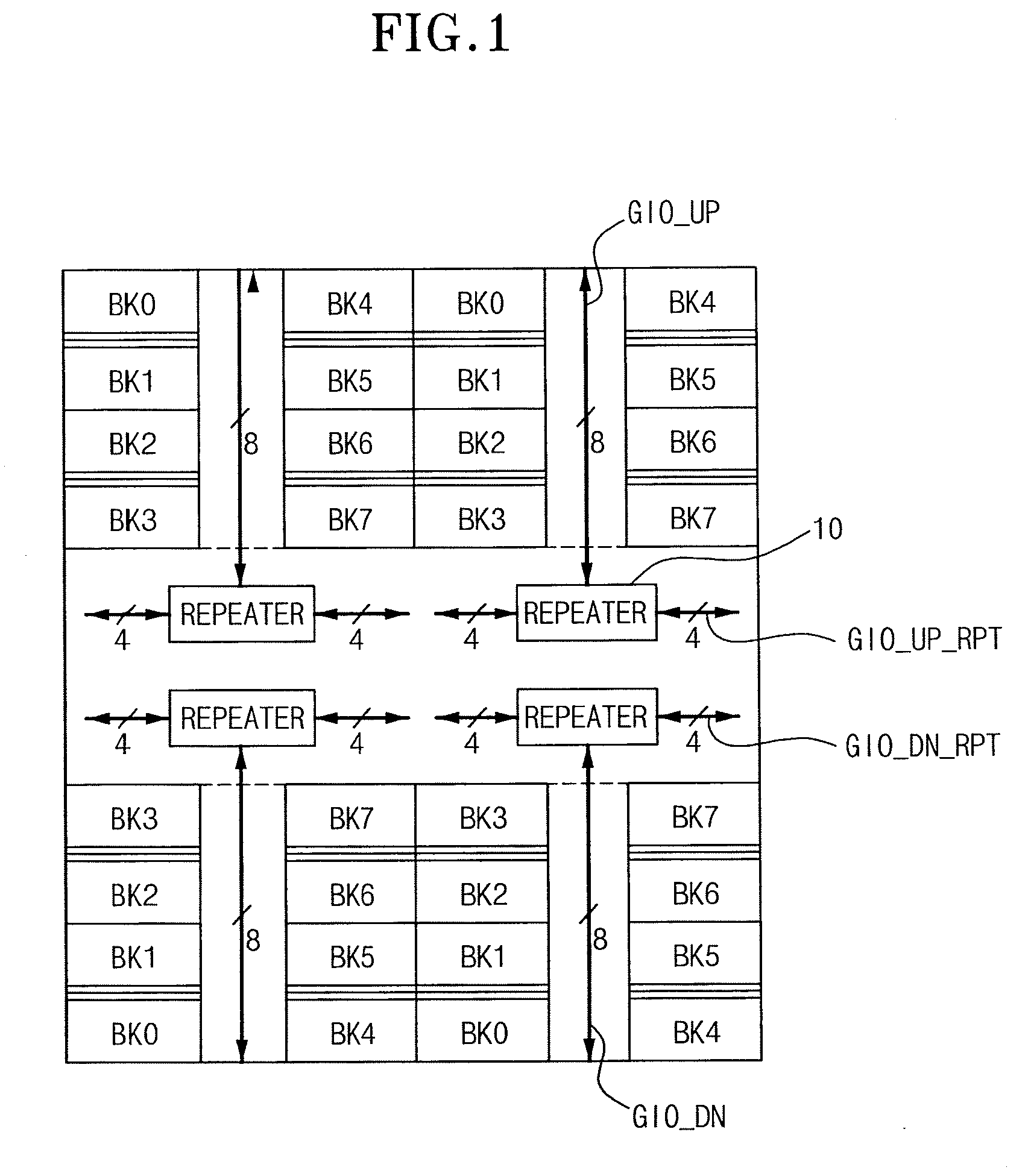
[0068]A preferred embodiment of the present invention is directed to a semiconductor memory device structured such that each bank is dividedly disposed in at least two regions, and the banks divided in each region are divided into groups so as to share a single global input / output line per a group, and is characterized by selecting the corresponding global input / output line in a read operation or a write operation and to deliver data via the selected global input / output line.

[0069]More specifically, considering a half-bank structure as shown in FIG. 3 as an example, an embodiment of the present invention is structured such that each bank BK0˜BK7 is dividedly disposed into two regions in the case of a 8-bank BK0˜BK7 structure with the number of input / output pads (not shown) being 32. Each bank BK0˜BK7 is dividedly disposed into two regions, the hal...


PUM


Abstract

A semiconductor memory device includes an input/output line of a data transfer path and its surrounding circuits, comprising a controller which generates a control signal corresponding to command and address input in read and write operation; and a repeater which selects any one of the plurality of bank groups as the control signal to control data transfer between the selected bank group and an input/output pad.

Description

CROSS-REFERENCE TO RELATED APPLICATIONS[0001]The present application claims priority to Korean patent application numbers 10-2007-0029686 filed on Mar. 27, 2007 and 10-2007-0029687 filed on Mar. 27, 2007, which is incorporated herein by reference in its entirety.BACKGROUND OF THE INVENTION[0002]The present invention relates to a semiconductor memory device, and more particularly to a semiconductor memory device including a global input / output line of a data transfer path and its surrounding circuits.[0003]In general, prior semiconductor memory devices, such as Graphic DDR SDRAM, have a quarter-bank structure as shown in FIG. 1 for high-speed operation.[0004]More specifically, referring to FIG. 1, in the case of an 8-bank (BK0˜BK7) structure, each bank BK0˜BK7 is dividedly disposed into four regions, in which input / output pads (not shown) and repeaters 10 are disposed between quarter banks BK0˜BK7 in an upper portion and quarter banks BK0˜BK7 in a lower portion.[0005]Global input / out...

Claims


Application Information

Patent Timeline
IPC IPC(8): G11C7/00G11C8/00
CPCG11C7/1048G11C7/1051G11C7/1069G11C7/1078G11C7/1096G11C8/08G11C8/14
Inventor PARK, KI CHON
Owner SK HYNIX INC
Why Eureka
Try Eureka