
Semiconductor memory device capable of controlling tAC timing and method for operating the same

Inactive Publication Date: 2008-10-02
SK HYNIX INC
View PDF17 Cites 9 Cited by
  • Summary
  • Abstract
  • Description
  • Claims
  • Application Information

AI Technical Summary

Benefits of technology

[0010]An embodiment of the present invention is directed to providing a semiconductor memory device capable of controlling a tAC with facility. A

Problems solved by technology

Recently, the operating speed of the data processing unit is getting faster and faster in the engineering development process of the semiconductor integrated circuits; however, the semiconductor memory devices to deliver the data to the data processing unit is not in compliance with the input and output speed of the data processing unit.
However, since the synchronous memory devices are unable to follow the operating speed of the data processing unit, DDR synchronous memory devices have been developed.
However, the system clock signal inputted into the semiconductor memory device reaches to a data output circuit, inevitably having a delay time which is caused by both a clock input buffer disposed within the memory device and a transmission line to transmit the clock signal thereto.
However, this causes a mismatch of a timing required to process the data to be outputted therein.
As a result, there is a problem in that the data are not outputted at a predetermined timing.

Method used


Image

  • Semiconductor memory device capable of controlling tAC timing and method for operating the same
  • Semiconductor memory device capable of controlling tAC timing and method for operating the same
  • Semiconductor memory device capable of controlling tAC timing and method for operating the same

Examples


first embodiment

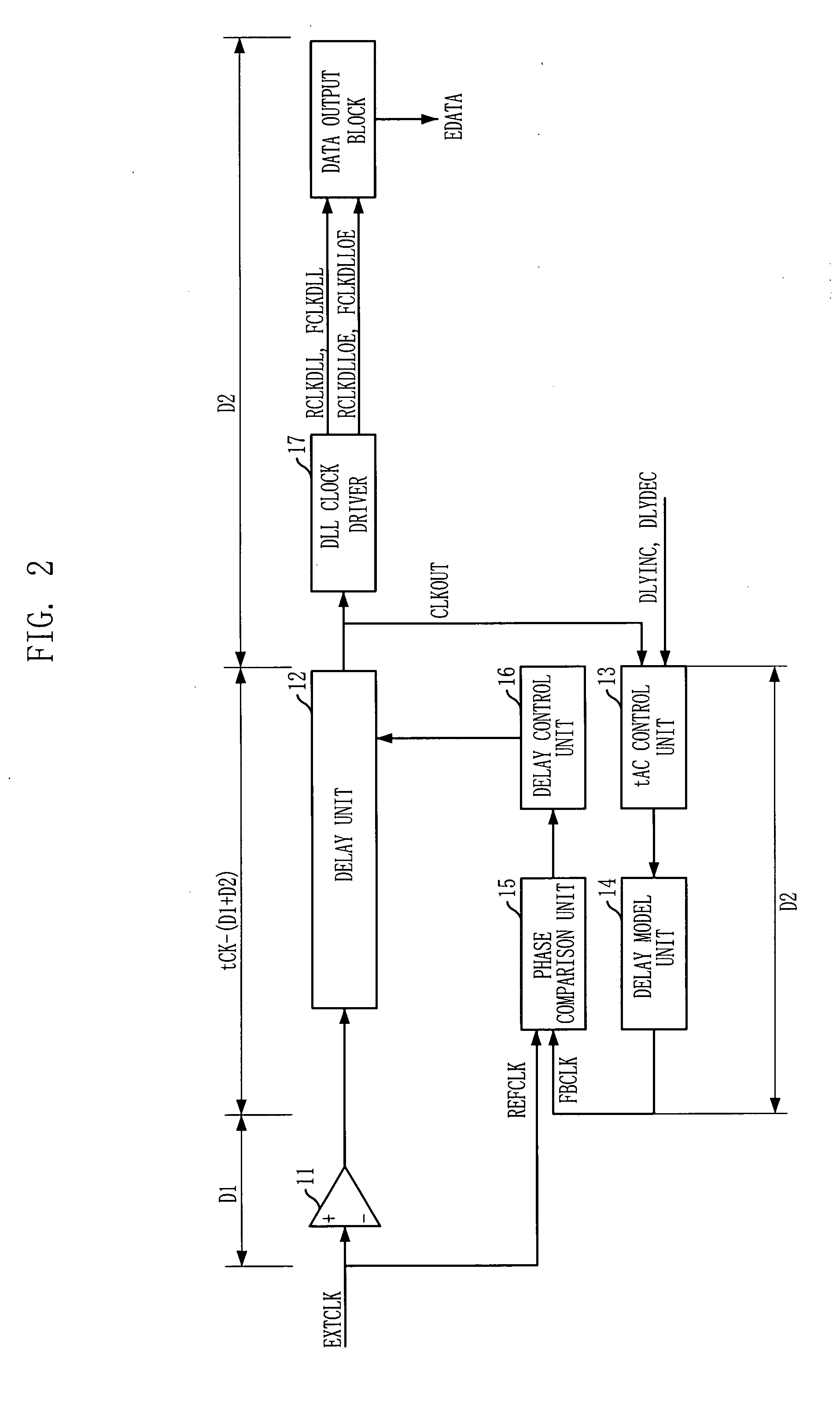
[0040]FIG. 5 is a block diagram illustrating the semiconductor memory device according to the present invention. The semiconductor memory device includes a delay locked loop circuit 100, a tAC control unit 100A, a data output block 1000 and a reference clock generating unit 2000. The data output block 1000 includes a data output timing control unit 1100, a data latch unit 1200, a data strobe signal generating unit 1300 and a data output unit 1400.

[0041]The delay locked loop circuit 100 produces a first delay locked clock signals RCLKDLL and FCLKDLL and a second delay locked clock signals RCLKDLLOE and FCLKDLLOE. The tAC control unit 100A outputs a delay-adjusted clock signals RDLL and FDLL by controlling the delay value of the first delay locked clock signals RCLKDLL and FCLKDLL in response to a control signals DLYINC and DLYDEC. The tAC control unit 100A is provided to adjust the tAC timing. The tAC control unit 100A controls the output timing of the data outputted from the data ou...

second embodiment

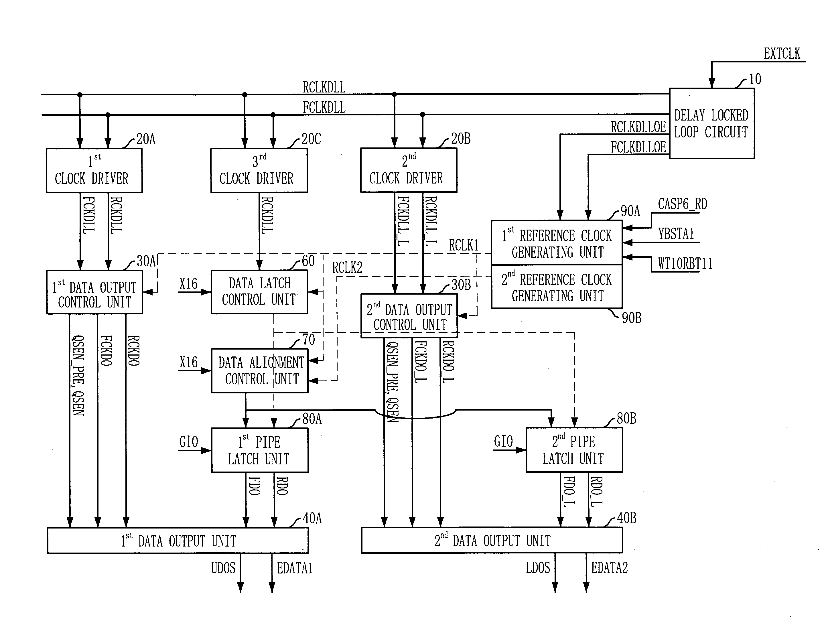
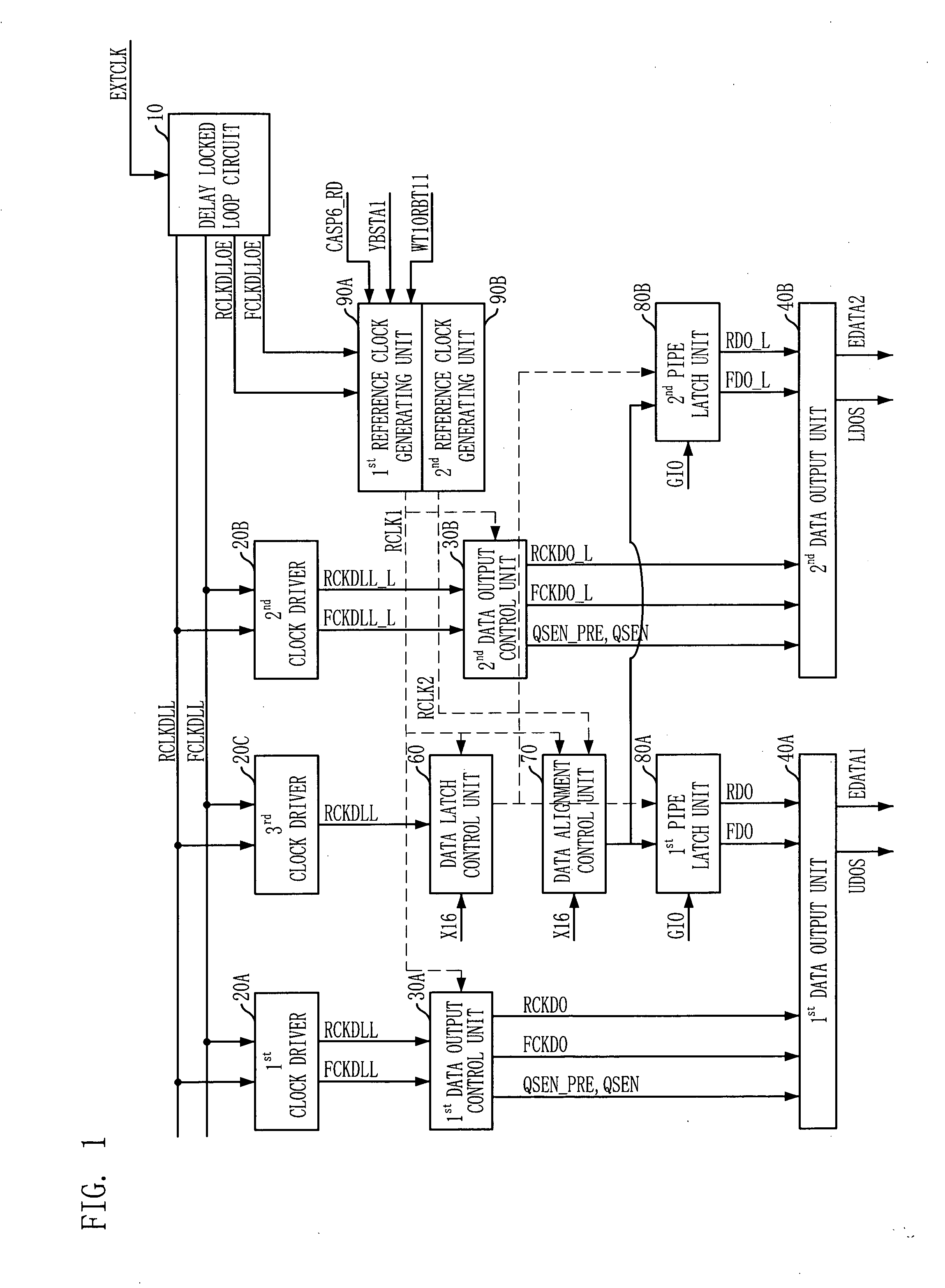
[0045]FIG. 6 is a block diagram illustrating a semiconductor memory device according to the present invention. The semiconductor memory device includes a delay locked loop circuit 100, a tAC control unit 100A, first to third clock drivers 200A to 200C, first and second data output control units 300A and 300B, first and second data output units 400A and 400B, a data latch control unit 600, a data alignment control unit 700, first and second pipe latch units 800A and 800B, and a first and second reference clock generating units 900A and 900B. Since the circuit blocks illustrated in FIG. 6 performs the same operation as those illustrated in FIG. 1, the detailed description related to these blocks will be omitted. The tAC control unit 100A controls the delay value of the first delay locked clock signals RCLKDLL and FCLKDLL and then outputs delay-adjusted clock signals RDLL and FDLL.

[0046]Moreover, the first and second clock drivers 200A and 200B and the first and second data output cont...

third embodiment

[0049]FIG. 9 is a block diagram illustrating a semiconductor memory device according to the present invention. The semiconductor memory device illustrated in FIG. 9 is characterized in that a data latch timing control unit 100C is additionally included in the semiconductor memory device of FIG. 6. The data latch timing control unit 100C controls the delay value of the second delay locked clock signals RCLKDLLOE and FCLKDLLOE outputted from the delay locked loop circuit. In this way, the processing timing and the output timing of data can be optimally maintained by differently controlling the delay values of the first delay locked clock signals RCLKDLL and FCLKDLL and the second delay locked clock signals RCLKDLLOE and FCLKDLLOE.

[0050]As apparent form the above, in the present invention, the operation margin for processing the output data is sufficiently obtained and the tAC timing is effectively adjusted. Therefore, the semiconductor memory device according to the present invention ...


PUM


Abstract

A semiconductor memory device is capable of controlling a tAC with a timing margin in an output data process. The semiconductor memory device includes a delay locked loop circuit, a tAC control unit, a reference signal generating unit, and a data output block. The delay locked loop circuit produces delay locked clock signals through a delay locking operation. The tAC control unit adjusts a delay value of the delay locked clock signals in order to control a tAC timing, thereby generating output reference signals. The reference signal generating unit produces a latch reference signal in response to the delay locked clock signals. The data output block latches data in response to the latch reference signal and for outputting the latched data in response to the output reference signals.

Description

CROSS-REFERENCE TO RELATED APPLICATIONS[0001]The present invention claims priority of Korean patent application no. 10-2007-0030768, filed in the Korean Patent Office on Mar. 29, 2007, which is incorporated by reference in its entirety.BACKGROUND OF THE INVENTION[0002]The present invention relates to a semiconductor memory device; and, more particularly, to a data output circuit in a semiconductor memory device.[0003]In a system equipped with a plurality of semiconductor devices for performing various functions, a semiconductor memory device functions as an apparatus for storing data. The semiconductor memory device outputs data, which correspond to the address signals inputted from a data processing unit, for example, a central processing unit, to a device to request the data, or stores data delivered by the data processing unit in unit cells corresponding to the address signals which are inputted together with the data.[0004]The operating speed of the system is getting faster and ...

Claims


Application Information

Patent Timeline
IPC IPC(8): H03D3/24
CPCG11C16/32H03L7/0812H03L7/0816G11C7/10G11C7/22G11C8/00
Inventor KIM, KYOUNG-NAMCHO, HO-YOUB
Owner SK HYNIX INC
Features
  • Generate Ideas
  • Intellectual Property
  • Life Sciences
  • Materials
  • Tech Scout
  • Unparalleled Data Quality
  • Higher Quality Content
  • 60% Fewer Hallucinations
Learn More